AGC can make through vias in thin glass substrate by the patterns of customers’ requirements. AGC expects TGV substrate in the use of 3D integration for semiconductor packaging, and other wide variety of fields.
Applications
- Substrate for Semiconductor Packaging and Glass Interposer
- 3D Glass IPD
- MEMS, Sensor Device
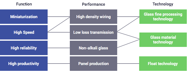
For the more connected world, we contribute to the miniaturization and acceleration of electronic devices through glass.
Features
- Miniaturization
- It enables micro wiring with excellent flatness, shape stability, and through fine via of the glass.
- High speed
- It enables high speed and large capacity communication with excellent high frequency properties, through high insulation and low dielectric loss tangent of the glass.
- High reliability
- It is best suited to the semiconductor packaging with non-alkali glass and coefficient of thermal expansion close to Si.
- High productivity
- It can support a wafer, as well as a panel size.
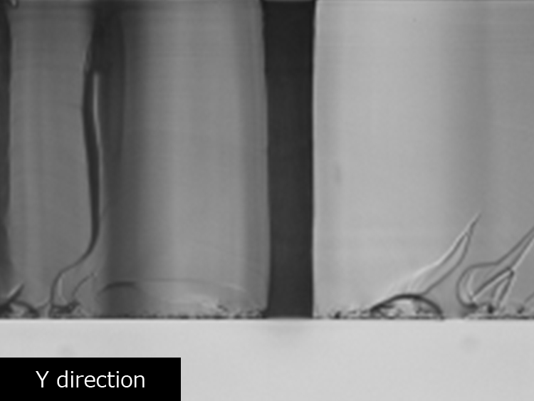
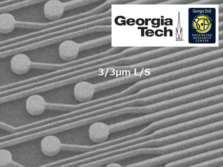 Micro wiring on glass
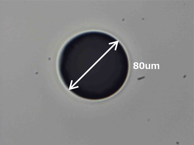
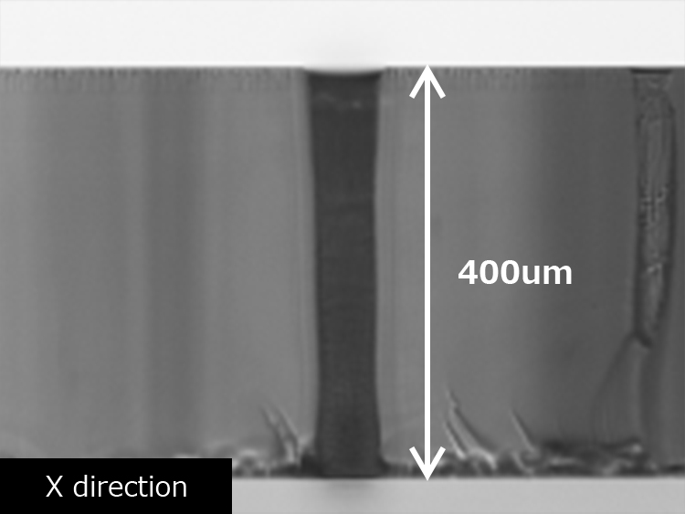
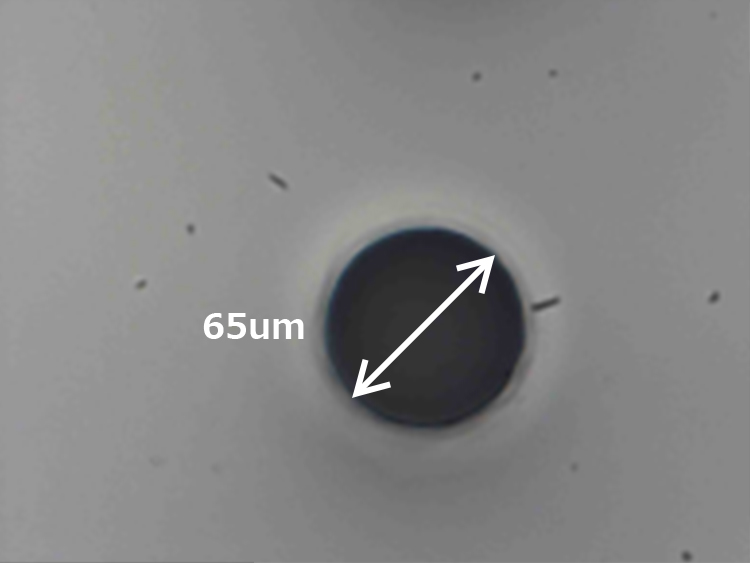
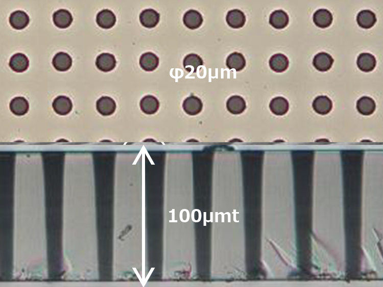 Micro processing of through glass vias
 “Wiring glass substrate for 3D integration” Courtesy of Fraunhofer IZM
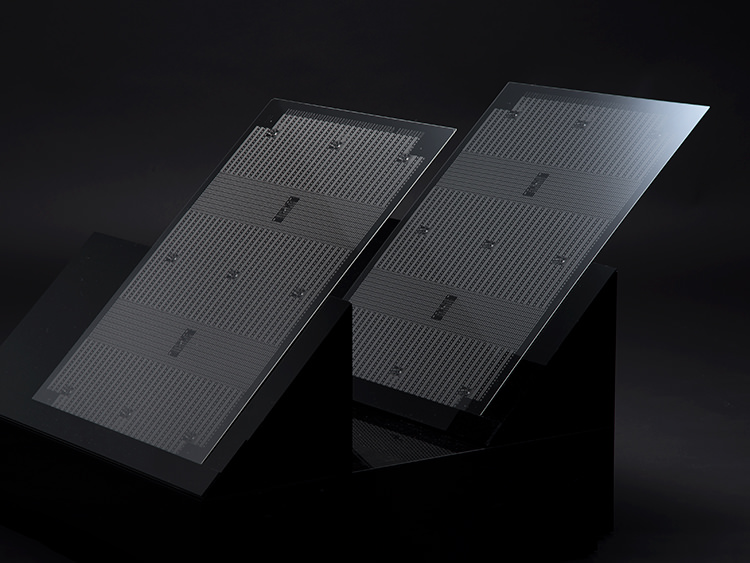
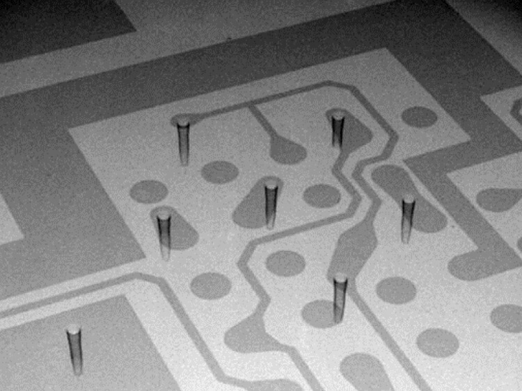
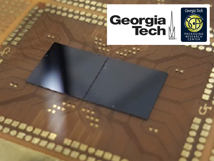 Glass Interposer
AGC delivers an excellent function to everyone through the performance on the basis of proven technologies.
Basic specifications
| Glass material | EN-A1 (Non-alkali glass) |
| Size | Wafer: φ150mm, φ200mm, φ300mm |
| Panel: ~550x650mm (Gen.3) | |
| Sheet thickness | 0.1mmt~0.5mmt |
| Hole type | Through Via, Blind Via |
| Hole shape | Straight, Taper, Hourglass |
| Hole diameter | φ20μm~φ150μm |
| Pitch | MIN. hole diameter × 2 |