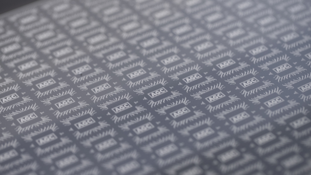
AGC’s Semiconductor Solutions Pioneering the Future of AI
With the rapid advancement and widespread adoption of AI, semiconductors that power computational processing face unprecedented demands for speed and energy efficiency. AGC contributes to the evolution of semiconductors by combining its unique material technologies with cutting-edge processing and surface functionalization.
At CES, AGC will showcase diverse solutions such as "Optical Waveguides" for next-generation optical interconnects and "Glass Cores" for high-density packaging—key innovations for the AI era. Discover how AGC’s materials support the very core of semiconductor technology.

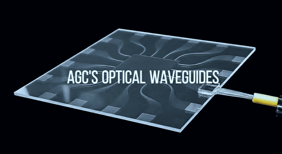

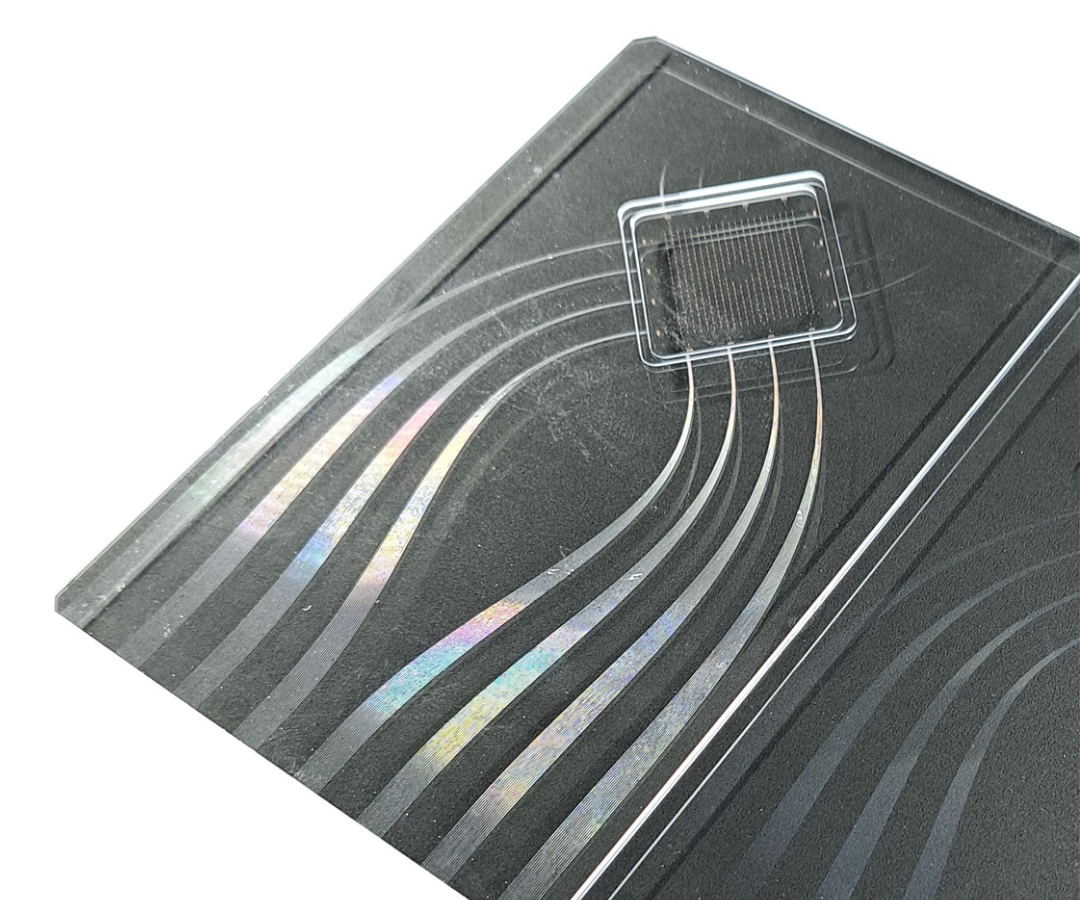
Optical Waveguide
Polymer and Glass Optical Waveguide (PWG and GWG)
PWG and GWG have the following features:
- High transmittance (O-band/C-band)
- Reflow compatibility / high-power laser durability
- Fine patterning by photolithography
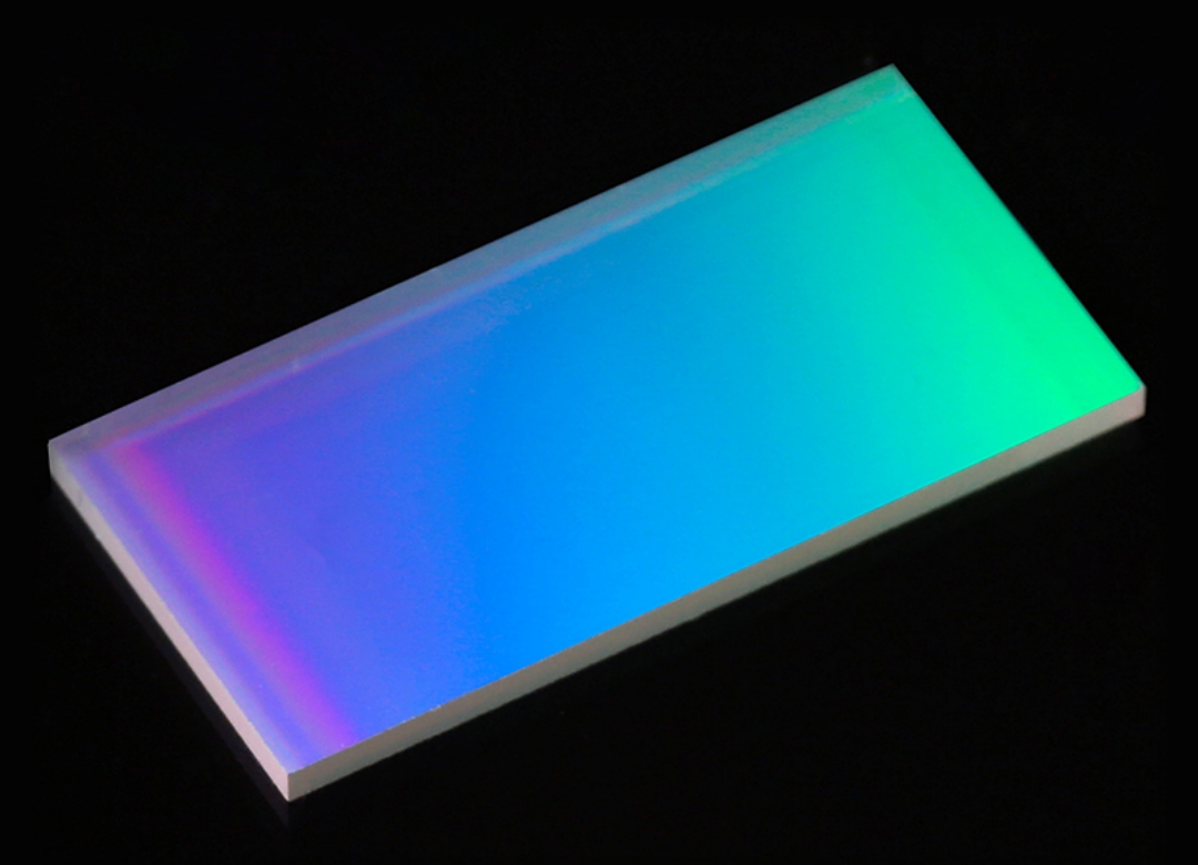
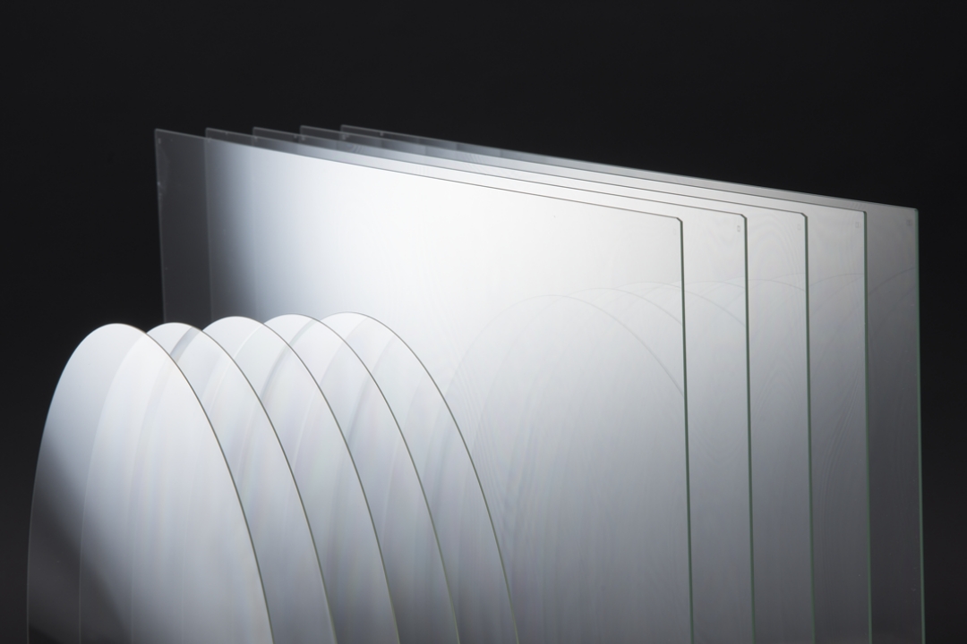
Glass Core / Interposer
TGV Glass Substrate for Advanced Packaging
AGC can make through glass vias (TGV) in glass substrates according to customers’ drawing and requirements. These TGV substrates can be used for 3D integration in advanced semiconductor packaging such as Chiplet , CPO substrate and RF devices.
- Available in a wide variety of glass compositions and thickness (0.1~1.1mm and over)
- High modulus for warpage control and CTE adjustability for stress optimization
- Precise fine pitch small TGVs (≧50μm), larger through and blind cavity formation possible
- High aspect ratio (up to 20:1 at 1.0mmt)
- Panel format production (e.g. 510x515mm)
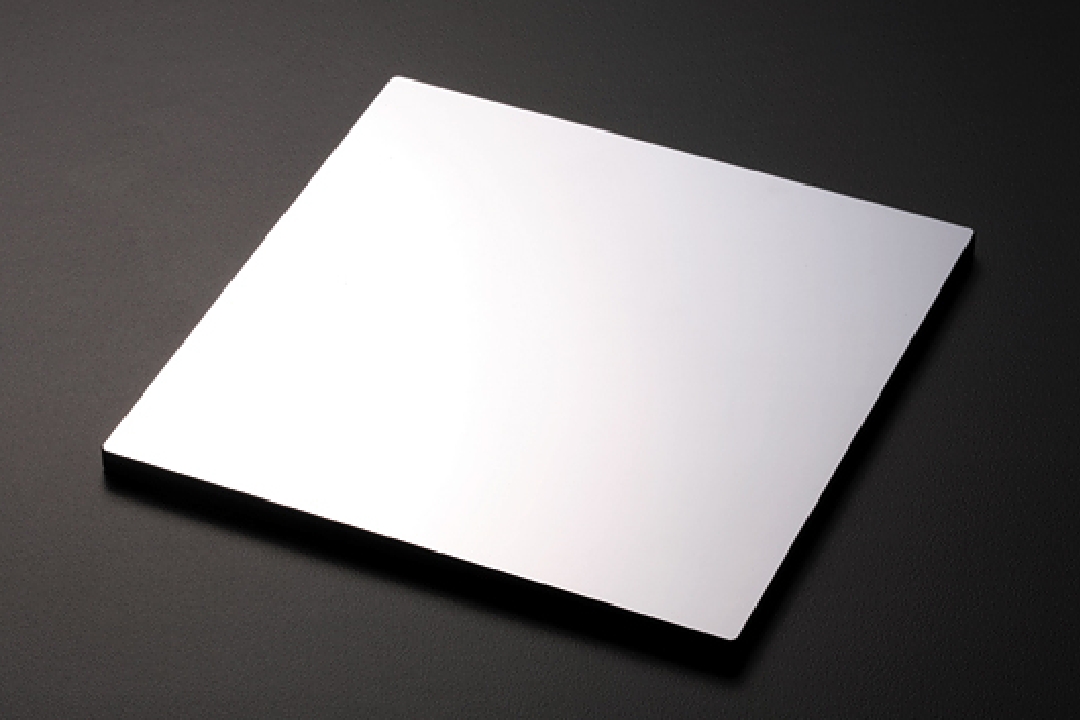
Copper Clad Laminate (CCL)
CCL has the following features:
- Extreme low loss (Df < 0.001)
- Stable dielectric performance over a wide frequency & temperature range
- Prepreg and laminated constructions
Mold Release Film
Fluon® ETFE FILM
Fluon® ETFE FILM is a high-performance fluoropolymer film. Fluoropolymer films are used in an extensive range of applications around the world because of its good properties including heat-resistance, chemical resistance, weatherability, optical transparency, non-adhesiveness, and electrical insulation. Fluon® ETFE Film has the following features:
- Non-adhesiveness
- Heat and chemical resistance
- Light transmittance, Weatherability
Silica Fillers for Electronic Use / Low Dielectric Underfill
There are two types of silica fillers: Hollow Silica (HS Series) and Solid Silica (HNP Series).
- HS Series: Low dielectric constant (Low Dk)
- HNP Series: Low dielectric loss tangent (Low Df)
We are also developing low dielectric underfill materials utilizing the above silica fillers.