

AGC Research Report 76(2026)
All glass metalenses with deep glass etching technique
Akira Ueno*, Fan Yanga*, Kohei Sano*, Yusuke Kataoka*, Akio Suguro* and Yasuo Hayashi*
* Innovative Technology Laboratories, AGC Inc., Yokohama, Japan
Abstract
Owing to their use of subwavelength nanostructures, metalenses show superior capability to replace conventional refractive counterparts. However, their applications at visible wavelengths are limited owing to restrictions in material choice and fabrication technique, making it challenging to design metalenses with high efficiency, large scale, and low fabrication cost simultaneously. To address this issue, we developed a single-step, rapid, and high-aspect-ratio glass-etching technique using catalysts for all-glass visible metalenses. By using the etching technique, SiO2 meta-atom pillars with an aspect ratio of more than 20:1can be achieved, which ensures sufficient optical phase coverage given the low refractive index of the glass. To demonstrate the capability of the technology, we designed and fabricated a 405 nm blue-light metalens, which has a 4 mm diameter and shows 69 % focusing efficiency. The same fabrication technique applies to green and red metalenses. Combining the RGB metalenses in a single device demonstrates the potential for full-visible-band, full-color imaging and virtual-reality applications. This report introduces the catalyst-based glass-etching technology and design schemes for prototyping metalenses.
Keywords: metalens, glass, visible band, HF-glass etching
1. INTRODUCTION
Metasurfaces with flat, engineered arrays of nanoscale elements are rapidly transforming optical design by enabling unprecedented manipulation of light within ultrathin form factors. Their versatility in controlling parameters such as wavefront, intensity, and polarization opens doors for new generations of lensing, beam-shaping, andmultifunctional photonic devices.1-4 Despite remarkable progress, much of the metasurface field remains reliant on high-index thin-film materials like amorphous silicon5-11, which are well-suited for infrared operation but often present complications in the visible regime due to absorption losses and strict fabrication tolerances.
Given the demand for robust visible-light optics applicable to imaging and sensing, silica-based platforms have gained momentum due to their optical clarity and mechanical stability.12-17 However, the transition to low-index materials is nontrivial: silica’s refractive index imposes the need for deeper structures with increased aspect ratios, challenging established microfabrication approaches. Standard plasma etching techniques, while mature for microelectronics, struggle with hard mask erosion and non-vertical sidewalls when attempting to realize tall, high-resolution silica nanostructures, often compromising device efficiency and reproducibility.16-21
In response, our work explores a plasma-free, catalyst-enhanced etching process using atmospheric hydrogen fluoride (HF) gas and a novolac-based photoresist.22- 24 Unlike conventional vacuum-based etching, it promotes anisotropic material removal through surface catalysis, yielding vertical, smooth, and deep features in SiO2 without the drawbacks of mask damage or ion-induced roughening. Computational insights from density functional theory (DFT) analyses reveal that the catalytic pathway reduces energy barriers, accounting for the experimentally observed selectivity and efficiency of the etch25.
Leveraging this innovative technique, we developed fused silica metalenses optimized for the blue light, which exhibits focusing efficiencies of 69 % with near-diffraction-limited performance, validating both the fabrication process and the viability of silica metalenses in the visible band26.
2. SiO2 ETCHING TECHNIQUE USING ANHYDROUS HF GAS AND A CATALYST
Achieving high-efficiency metalenses hinges on fabricating deeply etched, vertical nanostructures. This requirement is particularly demanding for SiO2 due to its low refractive index, which mandates deeper etch depths compared to metalenses based on higher-index materials such as Si3N427-29 or TiO230-33. Conventional ICP-RIE etching methods face significant obstacles when working with SiO2. The material’s poor selectivity relative to most mask materials necessitates the use of robust hard masks, typically metals like chromium or aluminum, but mask erosion during prolonged etch steps often leads to undesirable tapered profiles and undermines sidewall verticality16, 18. Moreover, plasma-driven processes can increase roughness and inflict substrate damage34, 35, further limiting the achievable performance and structural quality.
To overcome these challenges, we introduce a selective, plasma-free etching strategy that employs anhydrous HF gas together with a novolac-based photoresist acting as a catalyst22, 23. The procedure shown in Fig. 1 involves patterning a layer of novolac photoresist onto a SiO2 substrate using standard photolithography. The patterned substrate is subsequently exposed to heated, anhydrous HF vapor, which reacts preferentially with SiO2 at photoresist-covered sites. Once etching concludes, the catalyst resist is efficiently stripped away with oxygen plasma, restoring a clean etched surface. With exception of the HF vapor step, the entire process remains compatible with conventional semiconductor manufacturing and can be seamlessly adopted in existing fabrication facilities.
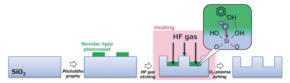 Fig. 1 Process flow of the etching technique using anhydrous HF gas and a catalyst. Enlarged view: schematic of the catalytic effect of a novolac polymer. Broken lines indicate interactions; red arrow shows the initiation of reactions.
A distinguishing aspect of this method is its site-selective etching mechanism. SiO2 alone shows almost no reaction with HF vapor under typical process temperatures (around 200–300°C) 22, 36; however, the presence of the novolac photoresist dramatically accelerates the local etch rate. This enhancement is attributed to the hydroxyl functional groups in the polymer, which catalyze the chemical exchange between the HF gas and the substrate. Density functional theory (DFT) modeling confirms that these hydroxyl groups participate in synergistic interactions both with hydrogen atoms in HF and with oxygen from the SiO2 matrix37, lowering the energy barrier for silicon–oxygen bond breakage and thus enabling rapid material removal. Importantly, the photoresist acts solely as a catalyst and is not consumed during the process, ensuring that the original pattern fidelity is preserved as the geometry is directly transferred into the underlying SiO2.
This approach offers several benefits. The catalyst-induced reaction produces sharply defined, vertical, and exceptionally smooth sidewalls regardless of etch depth, and the diffusion-driven nature of HF vapor ensures that even deeply etched profiles are accessible. Based on previous characterization of this etching technique22, 23, the fabricated structures are also expected to exhibit taper angles below 1° and sidewall roughness below 3–4nm, which are better than those typically obtained using conventional RIE techniques. Eliminating plasma from the process not only prevents plasma-induced defects but also obviates the need for both complex vacuum equipment and hard masks. Furthermore, since the process is compatible with batch operation, it supports scalable, high-throughput production at reduced fabrication costs.
3. METALENS CHARACTERIZATION
We designed and fabricated a metalens optimized to focus blue light at a wavelength of 405nm, using a hydrogen‑fluoride (HF) gas–catalyzed etching process. An optical‑microscope image of the patterned structure is given in Fig. 2a. Figs. 2b and 2c provide top and tilted view SEM images. The resulting meta-atom pillars exhibited a height of 1.8 μm and an aspect ratio of more than 20:1. This value falls below the design target, thereby introducing phase error into the metalens and resulting in a modest reduction in the measured efficiency relative to the theoretical maximum of 84 %. Given that a higher pillar height is associated with greater susceptibility to collapse, the selected etching thickness represents a compromise between metalens optical efficiency and mechanical robustness. With process refinement, we anticipate this gap can be minimized in future iterations. To further demonstrate our capability in fabricating ultra-thin metalenses, we fabricated a metalens sample using the same design and fabrication approach on a 0.1 mm fused-silica substrate. Fig. 2d shows a photograph of the completed sample, Fig. 2e presents a side-view comparison between the ultra‑thin metalens (left) and a similar metalens fabricated on a conventional 0.5 mm silica substrate (right), demonstrating the successful realization of the ultra‑thin platform without macroscopic damage or warping.
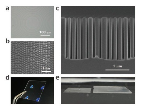 Fig. 2 Fabrication and structural characterization of the metalenses.(a) Optical microscope image and (b)top-view,(c) tilted-view SEM image of the 405 nm wavelength metalens.(d) Photograph of the metalens fabricated on an ultra-thin 0.1 mm glass substrate.(e)Side-view comparison between the ultra-thin metalens(left) and metalens on conventional 0.5 mm substrate(right).
For experimental validation, the metalens was evaluated using the setup depicted in Fig. 3a. An expanded blue laser beam was directed perpendicularly onto the metalens, and its focal spot was imaged and magnified using a microscope objective before reaching the power meter. Incident power over the lens area was gauged with a 4 mm pinhole matching the metalens aperture as illustrated in the small red box. To quantify performance, focusing efficiency is defined as the ratio of focal spot power (corrected for objective lens transmittance) to incident laser power through the pinhole. The metalens achieved a focusing efficiency of 69 ± 1 %, which is higher than those reported in previous studies under similar conditions16. Notably, adding an anti-reflection coating to the substrate is expected to further boost efficiency.
We then measured the point spread function(PSF) of the metalens by replacing the power meter with a high-resolution camera (Thorlabs CS165MU, 1440 × 1080 pixels, 3.45 μm pixel size). The experimentally observed focal spot is shown in Fig. 3b, with a full width at half maximum(FWHM) of 0.86±0.05 μm. The calculated Strehl ratio, normalized to the integrated power over a five-FWHM area, reached 0.76±0.03, indicating near diffraction-limited imaging performance. Fig. 3c compares the measured intensity profile across the X axis to the expected profile of an ideal lens with identical NA, showing close correspondence.
To assess imaging fidelity, we derived the modulation transfer function (MTF) from the PSF data via Fourier transform, which is shown in Fig. 3d. The MTF closely matches that of a diffraction-limited lens at the same numerical aperture, confirming both the high fabrication quality and the superior optical performance of the fabricated metalens.
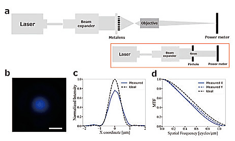 Fig. 3 Metalens optical measurement.(a) Efficiency measurement setup. Red box illustrates the incident power measurement setup.(b) Point-spread function (PSF)measurement.(Scale bar: 1 μm)(c) 1-D PSF along the horizontal direction.(d) MTF of the metalens.
4. CONCLUSION
In summary, we have established atmospheric HF-gas catalyst etching as a robust technique for crafting high-aspect-ratio, all glass metalenses and successfully addressed the challenge of achieving full phase modulation in low-index materials. The exceptional visible transparency of SiO2, coupled with the demonstrated fabrication precision, positions it as an ideal candidate for next-generation planar optics. Our prototype blue wavelength metalens achieved a substantial focusing efficiency of 69 % and delivered near diffraction-limited imaging, validating the approach’s practicality for high-performance devices.
This scalable fabrication process paves the way for large-area, broadband metalenses across the visible spectrum. The innovations have wide-ranging implications for advanced imaging, displays, augmented and virtual reality, biophotonics, and integrated optical systems. Overall, our results highlight the potential of all-glass metalens optics for emerging photonic applications requiring both visual clarity and manufacturability.
REFERENCES
- Chen, H. T., Taylor, A. J., & Yu, N.(2016). A review of metasurfaces: physics and applications. Reports on progress in physics, 79 (7), 076401.
- Hsiao, H. H., Chu, C. H., & Tsai, D. P.(2017). Fundamentals and applications of metasurfaces. Small Methods, 1 (4),1600064.
- Li, A., Singh, S., & Sievenpiper, D.(2018). Metasurfaces and their applications. Nanophotonics, 7 (6), 989-1011.
- Hu, J., Bandyopadhyay, S., Liu, Y. H., & Shao, L. Y.(2021). A review on metasurface: from principle to smart metadevices. Frontiers in Physics, 8, 586087.
- Hu, T., Zhong, Q., Li, N., Dong, Y., Xu, Z., Fu, Y. H., ... &Singh, N.(2020). CMOS-compatible a-Si metalenses on a 12-inch glass wafer for fingerprint imaging. Nanophotonics, 9(4), 823-830.
- Baek, S., Kim, J., Kim, Y., Seok Cho, W., Badloe, T., Moon,S. W., ... & Lee, J. L.(2022). High numerical aperture RGB achromatic metalens in the visible. Photonics Research, 10 (12), B30-B39.
- Zhang, L., Chang, S., Chen, X., Ding, Y., Rahman, M. T.,Duan, Y., ... & Ni, X.(2022). High-efficiency, 80 mm aperture metalens telescope. Nano letters, 23 (1), 51-57.
- Ueno, A., Lin, H. I., Yang, F., An, S., Martin-Monier, L.,Shalaginov, M. Y., ... & Hu, J.(2023). Dual-band optical collimator based on deep-learning designed, fabrication-friendly metasurfaces. Nanophotonics, 12 (17), 3491-3499.
- Yang, F., Lin, H. I., Chen, P., Hu, J., & Gu, T.(2023).Monocular depth sensing using metalens. Nanophotonics, 12(14), 2987-2996.
- Ranno, L., Yang, F., Romero, A. L., Lin, H. I., Zheng, H.,Yu, S., ... & Mendonca, C.(2024, October). Metasurface-enabled additive manufacturing via two photon polymerization. In Metamaterials , Metadevices , and Metasystems 2024 (Vol. 13109, pp. 40-45). SPIE.
- Yao, M., Zhu, Y., Ma, X., Yang, R., Wang, G., Luo, G., ... &Ke, Z.(2025). Design and fabrication of amorphous silicon-based metalens arrays for enhanced CMOS image sensors. Materials Research Innovations, 1-7.
- Stjernström, M., & Roeraade, J.(1998). Method for fabrication of microfluidic systems in glass. Journal of Micromechanics and Microengineering, 8 (1), 33.
- Hwang, J., Cho, Y. H., Park, M. S., & Kim, B. H.(2019).Microchannel fabrication on glass materials for microfluidic devices. International Journal of Precision Engineering and Manufacturing, 20 (3), 479-495.
- Li, Q., Wang, Y., Xue, Y., Qiao, L., Yu, G., Liu, Y., & Yu,S.(2022). Ultrasensitive analysis of exosomes using a 3D self-assembled nanostructured SiO2 microfluidic chip.ACS Applied Materials & Interfaces, 14 (12), 14693-14702.
- Cabeza, C., Rojas, F., Lobos-González, L., Lemaitre, D.,Villena, J., Cordero, M. L., ... & Ortiz, R.(2025). Capture and detection of extracellular vesicles derived from human breast cancer cells using a 3D self-assembled nanostructured SiO2 microfluidic chip. Journal of Biological Engineering, 19 (1), 1-17.
- Park, J. S., Zhang, S., She, A., Chen, W. T., Lin, P., Yousef,K. M., ... & Capasso, F.(2019). All-glass, large metalens at visible wavelength using deep-ultraviolet projection lithography. Nano letters, 19 (12), 8673-8682.
- Park, J. S., Lim, S. W. D., Amirzhan, A., Kang, H., Karrfalt,K., Kim, D., ... & Capasso, F.(2024). All-glass 100 mm diameter visible metalens for imaging the cosmos. ACS nano, 18 (4), 3187-3198.
- Li, Z., Campbell, S. D., Park, J. S., Jenkins, R. P., Lim, S. W.D., Werner, D. H., & Capasso, F.(2024). Heterogeneous freeform metasurfaces: a platform for advanced broadband dispersion engineering. arXiv preprint arXiv:2412.12028.
- Weigel, C., Brokmann, U., Hofmann, M., Behrens, A.,Rädlein, E., Hoffmann, M., ... & Sinzinger, S.(2021).Perspectives of reactive ion etching of silicate glasses for optical microsystems. Journal of Optical Microsystems, 1(4), 040901-040901.
- Martins, A., Contreras, T., Stanford, C., Tuzi, M., Albo, J.M., Escobar, C. O., ... & Guenette, R.(2024). High efficiency glass-based vuv metasurfaces. arXiv preprint arXiv:2401.11315.
- Pedersen, M., & Huff, M.(2017). Plasma etching of deep high-aspect ratio features into fused silica. Journal of Microelectromechanical Systems, 26 (2), 448-455.
- Sano, K. H., Ono, Y., Tobinaga, R., Imamura, Y., Hayashi,Y., & Yanagitani, T.(2024). Atmospheric gas-phase catalyst etching of SiO2 for deep microfabrication using HF gas and patterned photoresist. ACS Applied Materials & Interfaces, 16 (17), 22657-22664.
- Sano, K. H., Ono, Y., Tsukiyama, K., Nagai, S., Saito, A.,Hayashi, Y., & Yanagitani, T.(2025). Damage-Free Vertical Microfabrication of α-Quartz via HF Gas-Phase Catalyst Etching. ACS Applied Materials & Interfaces.
- 安田興平,林泰夫.(2025).フッ化水素ガスによるガラス表面への微細構造構築と濡れ性制御, AGC Research Report, 75.
- 飛永諒介.(2025).量子化学計算によるSiO2-HFガスエッチング触媒のメカニズム解析と網羅的探索手法の構築, AGC Research Report, 75.
- Ueno, A., Ono, Y., Yang, F., Sano, K., Kataoka, Y., Ebihara,Y. & Hayashi, Y.(2026) Glass based visible metasurfaces with deep glass etching technique. Proc. SPIE 13910,High Contrast Metastructures XV, 139100A.
- Zhu, Y., Liu, S., Chang, Y., Wang, Y., Zhou, S., Wu, C., &Liu, W.(2023). Broadband polarization-insensitive metalens with excellent achromaticity and high efficiency for the entire visible spectrum. Applied Physics Letters, 122 (20).
- McClung, A., Torfeh, M., Einck, V. J., Watkins, J. J., &Arbabi, A.(2024). Visible metalenses with high focusing efficiency fabricated using nanoimprint lithography. Advanced Optical Materials, 12 (9), 2301865.
- Zhang, Y., Jiang, X., Qu, G., Han, J., Li, C., Bo, B., ... & Xiao,S.(2025). On-chip integration of achromatic metalens arrays. Nature Communications, 16 (1), 7485.
- Khorasaninejad, M., Chen, W. T., Zhu, A. Y., Oh, J., Devlin,R. C., Roques-Carmes, C., ... & Capasso, F.(2016). Visible wavelength planar metalenses based on titanium dioxide. IEEE Journal of Selected Topics in Quantum Electronics, 23 (3), 43-58.
- Wu, Y., Yang, W., Fan, Y., Song, Q., & Xiao, S.(2019).TiO2 metasurfaces: From visible planar photonics to photochemistry. Science advances, 5 (11), eaax0939.
- Jung, D. E., Einck, V. J., Dawicki, A., Malgras, V.,Verrastro, L. D., Grosso, D., ... & Watkins, J. J.(2025). Full Wafer Scale Manufacturing of Directly Printed TiO2Metalenses at Visible Wavelengths with Outstanding Focusing Efficiencies. Advanced Materials, 2500327.
- Li, L., Pan, M., Zhang, J., Jiang, Y., Wang, S., Yang, P., ... &Hu, Y.(2025). Dielectric Metalens Array for Simultaneous Polarization and Wavefront Mapping in the Visible Spectrum. Nano Letters.
- Liying, W., Dan, L., Xiulan, C., Xueling, Q., Wenhao, Z., &Ling, M.(2024). Study of the fabrication technology on tapered structure in quartz. Optical Engineering, 63 (8),084103-084103.
- Ren, F., Pearton, S. J., Lothian, J. R., Abernathy, C. R., &Hobson, W. S.(1992). Reduction of sidewall roughness during dry etching of SiO2. Journal of Vacuum Science &Technology B: Microelectronics and Nanometer Structures Processing, Measurement, and Phenomena, 10 (6), 2407-2411.
- Ono, Y., Nagai, S., Hayashi, Y., Urashima, S. H., & Yui,H.(2023). The role of silanol groups on the reaction of SiO2 and anhydrous hydrogen fluoride gas. Journal of the American Ceramic Society, 106 (7), 4052-4060.
- RO Jones,(2015). Density functional theory: Its origins,rise to prominence, and future. Reviews of modern physics 87 (3), 897-923