Electronics
The dynamically changing electronics market. Technological innovation is accelerating in tandem with this dizzying pace. In such a world, there is a continuous demand for highly functional materials and components to be used in the next generation of products in the semiconductor field and in optoelectronics, smartphones, and tablets.
As the next generation high-speed communications is about to dramatically transform society, AGC is accelerating development by combining its marketing and technological capabilities to determine what materials and solutions are necessary to realize the next transformation.
Development story: Mask blanks for EUV exposure
AGC vertically integrated EUV mask blank technology and opened the way for practical application
AGC started its development of new materials and processes for EUV mask blanks, which are essential for production process of leading edge semi-conductor chips
Waves of technological innovations such as Big Data, A/I, High Speed Data Communication, VR, etc. are impacting industries across the boards. Semiconductor chips such as LSI and Ultra LSI play leading role of this series of technological innovations. It is said that rarity and impact to the advancement is once in 100 years scale. Due to their faster data process capabilities, higher data transmission capacities, and higher integration, electronic devices become more sophisticated and highly condensed. The trend will accelerate in each generation.
This evolution of such semiconductor chips is achieved by high level of miniaturization of semiconductor circuit patterns. Lithography technology is employed to make semiconductor circuit patterns by projecting circuit patterns fabricated on glass substrates called a photomask onto silicon wafers by means of the ultraviolet light. The theoretical limit of the circuit pattern size is considered to be 20 nm (nanometer, 1 nm = one billionth of a meter), and EUV (extreme ultraviolet) lithography technology, a semiconductor manufacturing process of the next generation, is essential in order to generate finer circuit patterns.
The conventional lithography uses the light of 193nm wavelength, which is called ArF lithography, and needs to be repeated multiple times to fabricate the circuit pattern with the size of 20nm or smaller. This leads to complicated and costly process. EUV, on the other hand, uses advanced light system with the 13.5 wavelength. It is 10 times shorter than the ArF lithography, and can achieve circuit patterns of 20 nm size or smaller at single scanning process.
AGC started research and development of mask blanks for EUV lithography technology in 2003. The advanced technology and quality control for synthetic quartz glass for semiconductors developed by AGC. It was recognized by International SEMATECH (present name: SEMATECH), an international semiconductor technology development consortium in USA, and AGC was asked participate in a project for mask blank development.
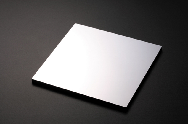
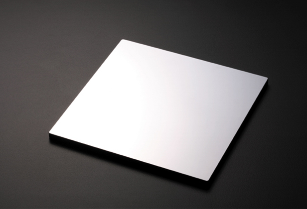
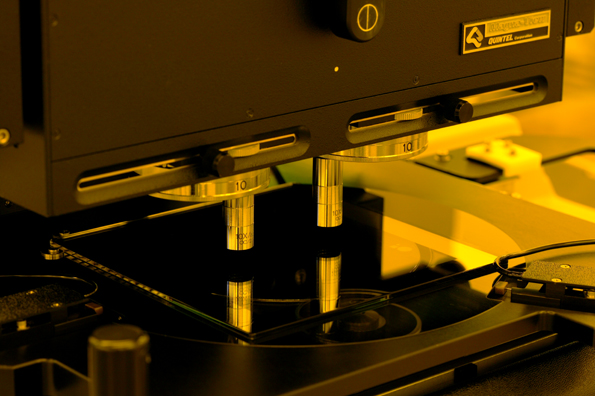
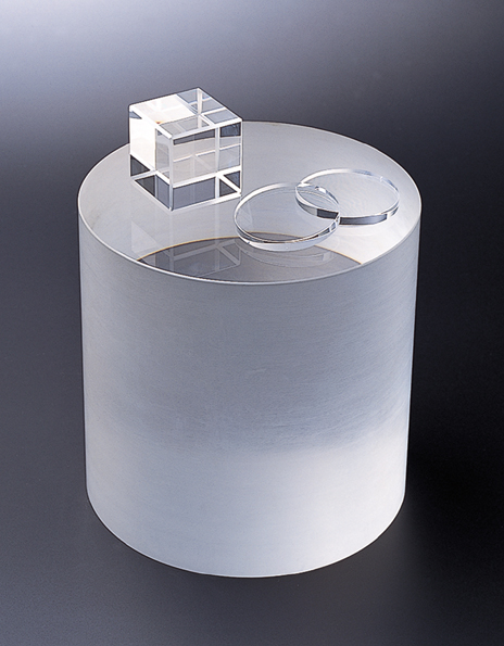
Mask blanks are base substrate plates of photomasks in which optical films of several compositions are deposited on the polished surface of low thermal expansion glass substrate. It is core technical aspect of EUV lithography technology. AGC has set a goal to become the one and only mask blanks manufacturer, which integrates technologies from glass material synthesis to polishing of the glass substrate and to film deposition.
The precision requirement for the EUV mask blank is 10 times tighter than the conventional mask blank of ArF lithography. It is mainly because the EUV lithography uses light of more than 10 times shorter wavelength than ArF lithography
AGC sent researchers to the mask blanks development center established by Sematech and its partners to conduct joint research. AGC also launched a project for developing our own process and material.
One of AGC researchers who participated in the research in the United States and became a driving force for the project states: "It started from scratch and required quality specification was so tight that I was not even sure if it would be possible. However, it was a great opportunity for AGC and it was also a challenging and interesting theme for an engineer. I dedicated all my strength to this project".
So, how tight was the required quality specification? The size of the blank was approx. 15 cm (6 inches). If the flatness of the surface of the blank is converted to a size of baseball park of 150 meter by 150 meter , the allowable peak-to-valley of the surface morphology would be less than 13.5 micrometers. On top of that, no foreign particles nor scratches as large as cedar pollen [to size of baseball park] was tolerated.
AGC also had to realize more than 50 kinds of qualities requirement from semiconductor manufacturers. It had to break through these "barriers" one by one to achieve commercial viability. Due to such difficulty in the development, AGC was unable to obtain single satisfactory glass substrate at the beginning.
The development schedule was originally 4 or 5 years to realize commercial viability, but was forced to postpone over and over mainly due to various external reasons. All the project members struggled as they could not tell when we could ever meet all technical requirements, and even if it could, we were not sure whether it could be commercialized. It was teamwork and resilience towards the development which empowered them in such a difficult time.
It was not a single innovative breakthrough which enabled us to put it into practical use. We solved each problem by analyzing its root cause, devising countermeasures and verifying their effectiveness repeatedly to demonstrate technical requirement. AGC also had to realize the required quality not by a single process, but by integrate multiple processes such as glass material production, glass polishing, wet cleaning, optical film deposition, etc. The team has passed the stringent quality requirements as each member fulfilled his/her own responsibility and passed the results to the next runner (process), like a long distance relay race.
On-time investment decisions backed up the development
It needs to be mentioned that the management team made on-time investment decisions to support the development team. Costly investments are usually approved after discussing them in many management conferences, and sometimes opportunities will be missed while waiting for the approvals. The time required for approval often determines whether the project succeeds or fails in the development of cutting edge technologies such as mask blanks in particular, therefore on-time investment decisions are required.
Behind such engagement, AGC has a consistent and strong determination to nurture in Electronics field as a pillar of the business. Such attitude of the management team motivates the development teams and became a driving force to advance development. The development of mask blanks is one of the examples.
Due to such efforts by the members, we saw the light at the end of tunnel around 2014 in the development. In response to this, AGC decided to greatly enhance the supply system in February 2018. If this business gets on track, AGC can not only demonstrate a great presence in the field of semiconductor manufacturing but also can greatly contribute to the development of the entire industry.
15 years have been passed since the development of EUV mask blanks started. The dream of the project members, who have devoted themselves to technological development under huge pressure, is finally becoming a reality.