July 27, 2020Products
AGC to Make Drastic Expansion to Supply System for EUVL Mask Blanks
AGC Inc. (AGC), a world-leading manufacturer of glass, chemicals and high-tech materials, has decided to drastically expand a supply system for EUV lithography photomask blanks ("EUVL mask blanks") at its group company, AGC Electronics Co., Ltd. (Headquarters: Koriyama, Fukushima Pref.; President: Hiromasa Sato). The construction including building expansion will start in coming October and operations are scheduled to start in 2022.
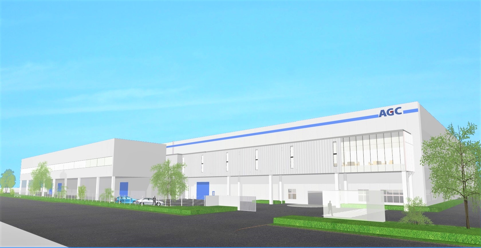 AGC Electronics new production facility (conceptual drawing)
AGC began conducting R&D on photomask blanks to be used as a consumable part for semiconductor production using EUV lithography technology in 2003. By combining its core technologies (i.e. glass materials, glass processing, and coatings), it continued technological development of photomask blanks and began production of EUVL mask blanks in 2017. AGC has made necessary investments to meet market demand, and to respond to further expansion of the EUV lithography market, AGC has decided on this drastic expansion of the supply system for EUVL mask blanks.
Notes
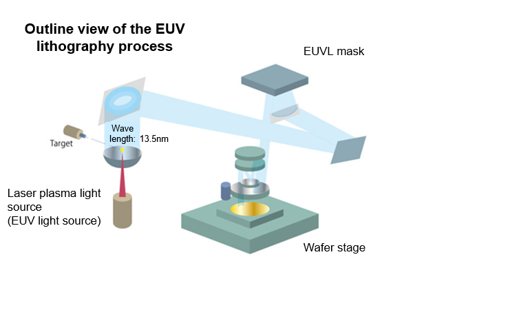
1: Optical Lithography Technology: The process of transferring LSI circuit patterns to silicon wafers, etc., using a KrF (krypton fluoride) or ArF (argon fluoride) light source. It is theoretically unrealistic to fabricate miniaturized patterns at what is commonly termed a "7nm" level.
2: EUV: Extreme ultraviolet radiation with a wavelength of 13.5nm.
- REFERENCE -
| Official name | AGC Electronics Co., Ltd. |
| Capital | 300 million yen |
| Representative | Hiromasa Sato |
| Head office location | Koriyama City, Fukushima Prefecture |
| Employees | Approximately 700 (as of the end of December 2019) |
| Primary business | Glass frit and paste for electronics, optoelectronics products for components such as optical pickups and synthetic silica glass for semiconductor manufacturing semiconductor-related materials business, optical device related business, EUV lithography photomask blanks, etc. |
EUVL mask blanks are a low-thermal expansion glass substrate with various kinds of optical coating films on its surface. An EUV photomask comprises a semiconductor chip circuitry pattern formed onto the surface of an EUVL mask blank, and this circuit is transferred onto a silicon wafer in order to create a semiconductor chip.
Due to the further miniaturization of circuits, EUVL mask blanks are increasingly expected to:
・ Have as close to zero micro-defects as possible;
・ Have almost perfect flatness
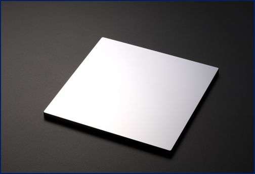 EUVL mask blanks
- MEDIA INQUIRIES
- Kazumi Tamaki, General Manager, Corporate Communications & Investor Relations Division
AGC Inc. - Contact: Momoyo Nakanishi
- TEL: +81-3-3218-5603
- E-mail: info-pr@agc.com