January 17, 2002Products
Increasing Production Capacity of large-sized TFT-LCD Glass Substrates
- Responding to growing demand for use in large LCD TV sets -
Tokyo, JAPAN - Asahi Glass Co., Ltd. (AGC, Head Office: Tokyo; President: Shinya Ishizu) announced today that it has succeeded in using a high-transparency fluoropolymer, a leading candidate for next-next generation photolithographic semiconductor manufacturing using F2 (fluoride dimer) excimer lasers, as a photoresist base polymer in a 250nm film (one nm, or nanometer, is 1/1,000,000,000 meters), to create the world's first 100nm-width fine pattern (1:1 line-and-space).
The company has been following the development roadmap agreed under the Project Asuka private-industry collaborative program with its theme of developing 0.07-micron line-width semiconductors (a micron, or µm, is 1/1,000,000 meters). AGC successfully developed, in February of 2001, a high-transparency fluoropolymer as a photoresist base polymer for use with F2 lasers. Subsequently, working with Selete (Semiconductor Leading Edge Technologies, Inc.), various evaluations of its viability as photoresist have been performed, including its development characteristics, resolution and suitability for dry etching and "spin-on" coating.
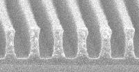
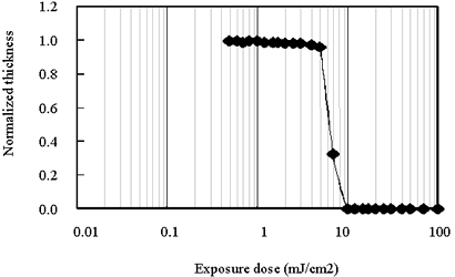
The most difficult technical challenge in the practical implementation was to use an F2 laser in actual photolithography to form fine patterns in resist coatings 200 to 300nm thick. AGC successfully designed and synthesized the new high-transparency fluoropolymer to achieve an absorption coefficient of less than 1.0 µm-1 for 157nm light. Since then, Selete has evaluated the new fluoropolymer as capable of forming a 100nm fine pattern in a practical 250nm coating (see accompanying photomicrograph). The fluoropolymer has an extremely high development sensitivity of less than 10mj/cm2 (mj = millijoule), confirming that it possesses most desirable characteristic for the formulation of highly sensitive photoresist materials (see accompanying figure).
AGC currently supplies industry with fluoropolymers including PTFE for semiconductor manufacturing facilities, and itself manufactures and supplies an 80% share of the transparent fluoropolymers for pellicles used in photo mask covers with KrF lasers. It has also begun high volume production of Cytop® for pellicles with next-generation ArF lasers. The company is exploiting its core capabilities in fluorochemical engineering to provide a wide lineup of fluoropolymers.
Worldwide demand for photoresist used in semiconductor manufacturing is put at 80 to 90 billion yen (6 to 7 billion US dollars) per year. AGC is working to provide timely samples to resist producers, production equipment manufacturers and device makers by boosting its prototype production facilities in time for spring, 2002, while simultaneously preparing to strengthen development work and expand production capacity in time for the expected start-up of F2 laser production in 2005 and for the roll-out of high-volume production in 2007.
For reference
|
1. |
Line and space |
|
2. |
Selete (Semiconductor Leading Edge Technologies, Inc.) |
|
3. |
The Asuka Project |
|
4. |
Development, resolution, sensitivity. |
|
5. |
Absorption cooefficient |
Photomicrograph : Profiles of 100nm and 95nm line-space patterns in 250nm film
(Levinsohn mask)
| 100nm L/S | 95nm L/S |
 |
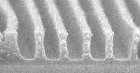 |
Figure : Degree of Development
Degree of Development : 10.0 mJ/cm2
- Contact :
- Asahi Glass Co., Ltd.
Mr. Akihiko Ninose
E-mail:info-pr@om.agc.co.jp
Corporate Communications Division
F a x : 81-3-3201-5390 - TEL: 81-3-3218-5915