December 24, 2003R&DOthers
Successful Development of New Next-Generation Non-Volatile Memory cell.
Asahi Glass Co., Ltd. (headquarters: Tokyo; President: Shinya Ishizu) and research group led by Koyanagi, professor of Graduate school of Engineering, Tohoku University, have succeeded in development of a new non-volatile memory, named Metal Nano Dot (MND) Memory (Fig.1,2). The MND memory is applied the deposition technology of MND film based on the synergy ceramic technologies possessed by Asahi Glass Co. As is shown in Fig.3, the MND film is composed extremely high dense metal nano dots embedded in insulating matrix. The MND memory is expected to be substituted for existing flash Memory in the near future.
While Asahi Glass Co. has leveraged the broad array of materials and technologies it has cultivated over many years, encompassing both inorganic and organic materials (such as glass, ceramics and chemical products), it develops, manufactures and markets semiconductor devices & materials. The new memory is an application of the formation technology on the ultra fine metallic structure embedded in insulator, which was derived through research into synergy ceramics, a national project in which Asahi Glass Co. has been involved.
Meanwhile, Professor Koyanagi has been engaged in design and fabrication of sub-micron semiconductor devices, one of the most famous researchers in the world. And his research group has obtained excellent results.
Demand to a high density and high performance non-volatile memory has rapidly grown as the market of mobile information devices has expanded in recent years, therefore many kinds of non-volatile memories have been proposed and investigated. Flash memory is the most widely used of the non-volatile memories, because of its high density, low manufacturing cost and stable operation and so on. However, it is said that scaling-down of the flash memory cell size has become more and more difficult because the tunneling oxide thickness can not be scaled down with the cell size due to keeping excellent charge retention and endurance. In order to solve this problem, new types of memory cells, such as silicon nano dots memory and MONOS memory, have been proposed. However, these memories do not have sufficiently high density of charge retention sites, therefore magnitude and uniformity of memory window are not enough. Professor Koyanagi paid attention to the MND film developed by Asahi Glass Co. to apply to new non-volatile memory, the MND memory, and has worked with Asahi Glass engineers on the trial devices. The fabrication of the trial devices was carried out at Venture Business Laboratory of Tohoku University.
The followings feature the MND Memory
| (1) | In the conventional flash memory cell and the silicon nano dots memory, floating gates retaining charges are made of silicon. On the other hand, in the MND Memory the MND film is used as charge retention layer, and each metal nano dot in the MND film works as a floating gate. The MND film consists of metal nano dots with diameter of around 2 nanometers dispersing at high density in insulator such as silicon dioxide (Fig. 3). Compared with the size and the density of the silicon nano dots conventionally studied, the size of the metal nano dots is about less than half, and the density is higher than 10 times, about 2 x 10¹³/cm2. These features enable to stabilize the memory operation due to wide and uniform memory window and also deliver on dramatic gains in long retention time and excellent endurance even in highly advanced scaling down device in future. |
| (2) | Since the sputtering method is applied to the MND film deposition, it can be formed readily and at low cost. The metal nano dot is formed self-organically in the insulating matrix, and the MND film grows with phase separating of metal and insulator. Therefore, no special treatment for formation of the metal nano dots, such as heating after film formation, is required. As characteristics of trial MND memory device with these remarkable features was successfully evaluated, it was highly attracted audiences' attention at the International Electron Devices Meeting 2003 held in Washington D.C. from December 8 to December 10. |
In the near future, Asahi Glass Co. intends to license the basic technologies on the MND Memory to semiconductor manufacturers, and hopes to increase the share in the existing flash memory market (1 trillion yen) and magnetic storage media market such as hard disk (2.6 trillion yen).
<Reference>
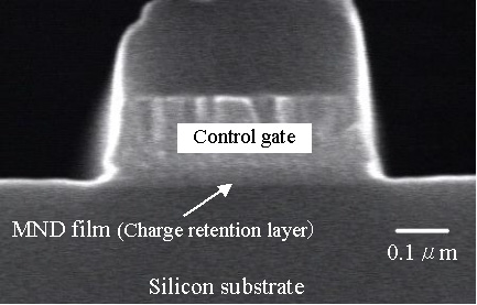 Fig. 1 Cross sectional SEM image of MND Memory cell. |
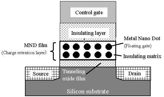 Fig. 2 Cross sectional diagram of MND Memory cell |
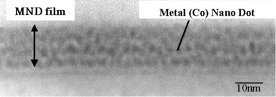 Fig. 3 Cross sectional TEM image of MND (Co/SiO2) film |
<Terms>
1. Synergy ceramics
The name of synergy ceramics is derived from Research & Development Program of Synergy Ceramics, the name of a project started in 1994 under the Research & Development System for Industrial Science and Technology, which was organized by Agency of Industrial Science and Technology of the then Ministry of International Trade and Industry (now the Ministry of Economy, Trade and Industry). The term of "synergy" denotes symbiosis and cooperative effects. The project aims to create revolutionary ceramic materials that allow for highly advanced symbiosis and the synergic effects of properties and functions (that are regarded as difficult to maintain concurrently), under the concept of "structural control at advanced dimensions," intended for controlling several structures of materials simultaneously.
2. Non-volatile memory
Non-volatile memory denotes semiconductor memory that retains stored data even power supply stops. ROM (Read Only Memory) is one of the non-volatile memories. In the narrow sense, it refers to ROM that allows writing and erasure, or flash memory.
3. Floating gate
Floating gate works as charge retention part in flash memory, electrically floating due to embedded in insulator between substrate and control gate.
4. Sputtering method
The sputtering method is that, ions are accelerated to hit target in plasma, and the sputtered atoms of the target are depositing on wafer.
5. International Electron Devices Meeting
Nicknamed the "World Cup of Semiconductor", the International Electron Devices Meeting is one of the most authoritative meeting on semiconductor in the world at which leading-edge device development results from around the world are carefully screened out and reported. It is held in December annually in the United States.
- For questions and comments on the subject, please direct your inquiries to:
- Shinichi Kawakami, Director, Corporate Communications Division, Asahi Glass Co., Ltd.
- Contact: Y. Saito
- TEL: 03-3218-5509
- E-mail: info-pr@agc.co.jp