Optical thin films have been widely used mainly as antireflection films for camera lenses and cold mirrors for lighting. In addition, the development of various lasers such as semiconductor and gas lasers has also led to the development of essential optical thin films such as laser mirrors and beam splitters. With the development of a deposition system and the application of ion processing and sputtering technology, optical thin films with high-precision optical properties and high durability have been produced. In the late 1990s, optical filters with more than 100 thin-film layers were manufactured and used as key components for optical communications. Today, they are used in advanced optical systems such as LiDAR for smartphones and automobiles and optical pulse measurement for wearable devices. Optical thin films are an essential technological element for the development of optoelectronics.
What is an optical thin film?
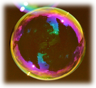
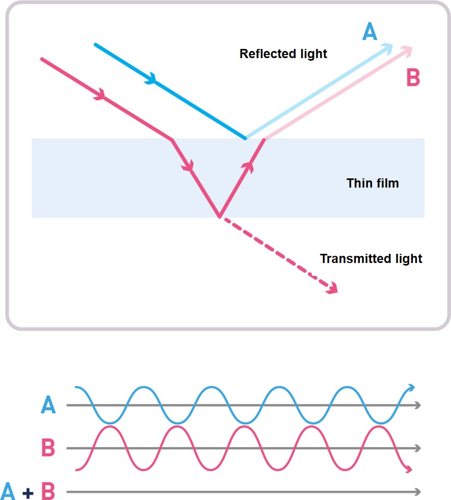
When light is incident on a thin film, interference occurs between the light reflected outside the film interface and the light reflected inside the film interface. The reason why soap bubbles and an oil film develop rainbow colors is that the interference conditions of light change as the thickness of the film constantly changes.
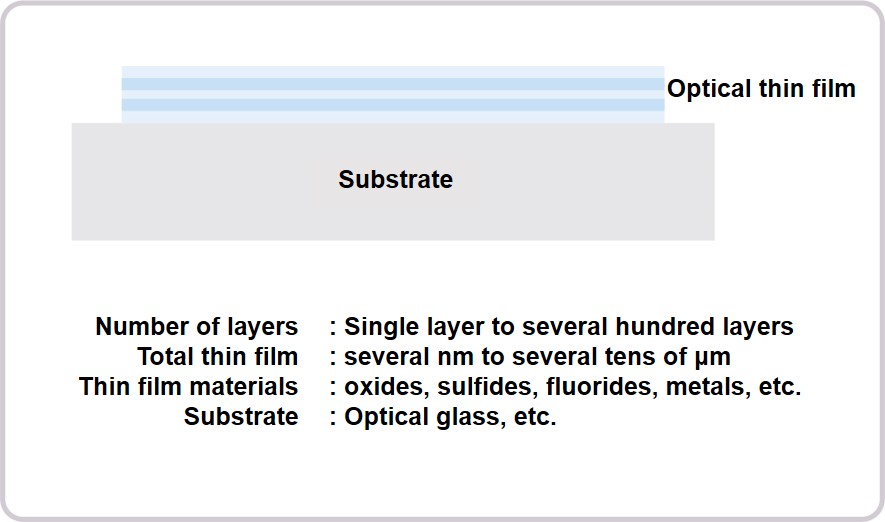
An optical thin film is a thin film that has unique optical properties (such as adjusting light intensity, allowing only selected wavelengths to pass, separating light components, or changing optical paths) using light interference conditions that can be controlled by arbitrarily designing the thickness, material, and number of layers of the film.
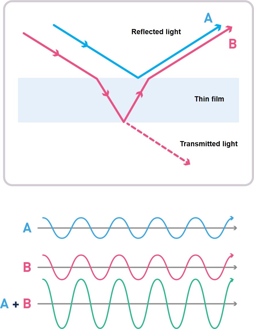
Optical thin films make use of the interference between light A reflected at the entrance plane and light B passing through the thin film and reflected at the exit plane.
For example, if the oscillations of A and B are similar, the oscillations cause interference (A + B) that amplifies the oscillations.
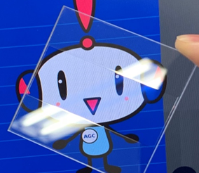
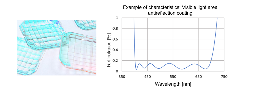
In the image on the left, an optical thin film called an antireflection coating is formed in the central zone of the glass.
At the interface, the reflected lights A and B interfere and cancel each other out, resulting in an infinite loss of reflected light and greater light transmission. The area without the antireflection coating reflects the fluorescent light, while at the central zone where the antireflection coating is formed it appears as if there is no glass there.
Optical thin films can be used not only for visible rays but also for ultraviolet and infrared wavelengths. They are used as optical elements for optical filters, laser mirrors, etc. in a wide range of fields such as automotive, medical, household electric appliances, and exposure light.
Manufacturing process of optical thin films
Thin film manufacturing processes can be broadly divided into vapor phase and liquid phase processes, and various methods have been developed. A vapor phase process is commonly used for optical thin film production.
This section introduces vapor deposition and sputtering, which are classified as physical vapor deposition (PVD) of the vapor phase process.
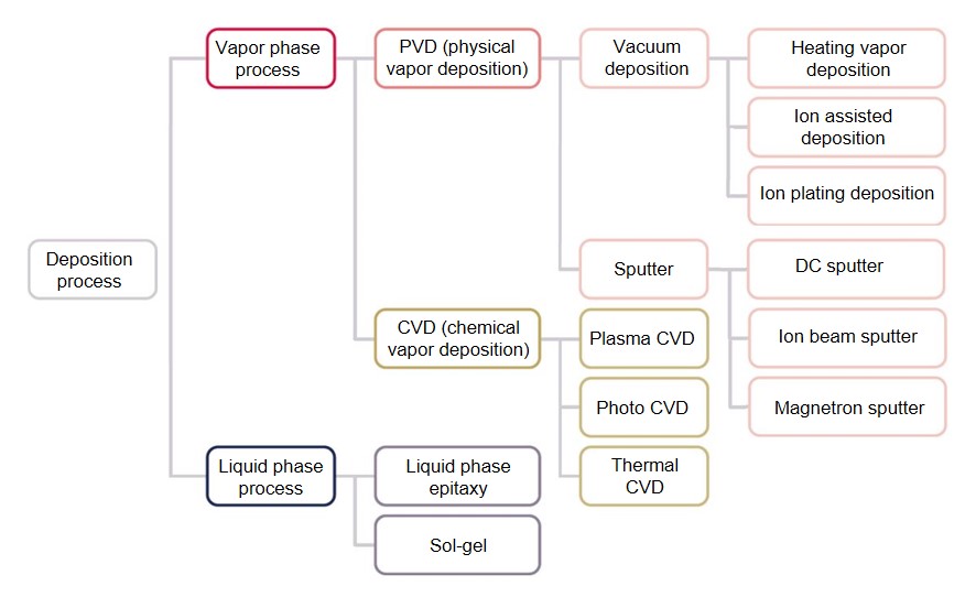
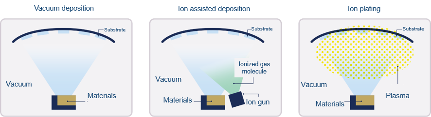
Vacuum deposition
Vacuum deposition is a deposition technology in which a material is heated and evaporated or sublimated into vapor in a vacuum and then the vapor is deposited onto substrate surfaces to form thin films. Materials can be heated either directly by an electron beam or indirectly by resistance heating. Vacuum deposition is a classic process, but it can also be used for dissociative substances such as fluoride, and is characterized by its high deposition rate.
Ion assisted deposition
Ion assisted deposition is a process in which ionized gas molecules are bombarded in the direction of vapor propagation during vacuum deposition, causing the vapor to accelerate and adhere onto the substrate with higher energy.
Ion plating deposition
Ion plating deposition is a process in which vapors are passed through the plasma and adhered onto the substrate. Vapors are partly ionized in the plasma, and deposited onto the surface with strong adherence strength by the sputtering effect of the plasma. Deposition processes that utilize the ionic force, as with ion assisted deposition and ion plating deposition, can deposit films with high density and high adhesion compared with deposition using only heating, and can produce highly reliable optical thin films without a wavelength shift.
Sputter
Sputtering is a process of depositing films in which the material (target) to be deposited is bombarded with ions such as argon ions or atoms in the plasma state to eject the target material. Compared with vacuum deposition in which the target material is heated and evaporated to deposit a thin film, the target molecules have higher energy in this method. This provides the film with higher adhesion strength, resulting in a dense thin film.
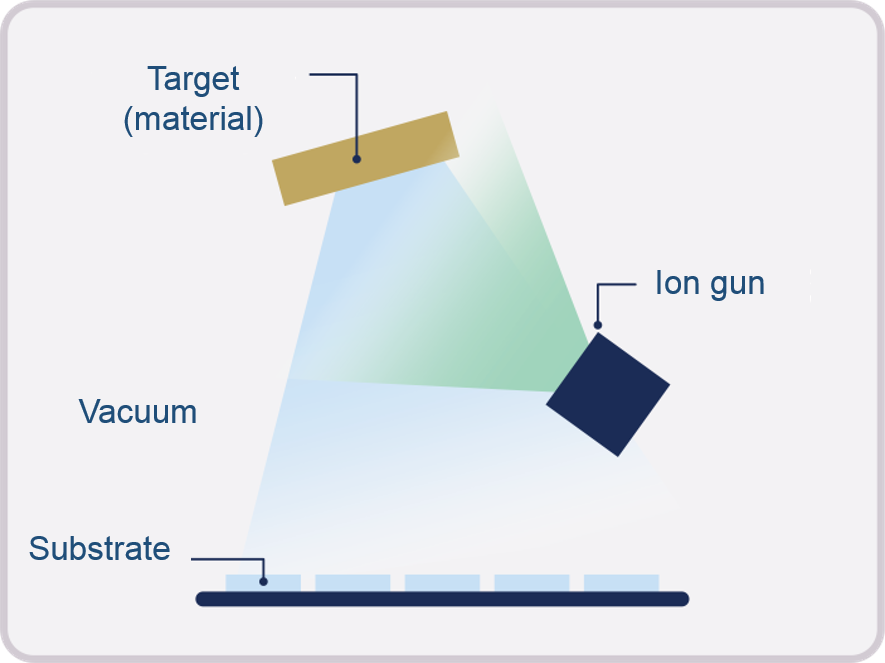
Ion beam sputter
Argon ions are ejected by applying a voltage to the ion gun (i.e. the sputtering source) from plasma generated by applying a high frequency to argon gas. The ejected argon ions collide with the target material and sputter the film material. By depositing a sputtered film material, an optical multilayer film can be formed.
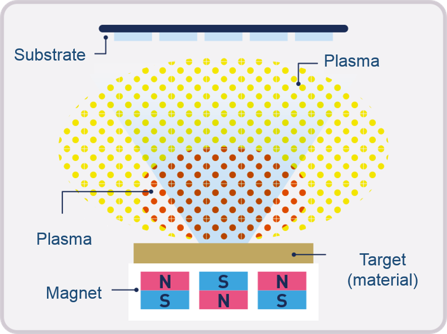
Magnetron sputtering
In magnetron sputtering, magnets are placed on the back of the target to generate a magnetic field that surrounds the electrons, creating a dense plasma region that can efficiently sputter the target. Unlike vapor deposition where the deposition source is a point, magnetron sputtering enables uniform deposition over a large area. Films formed by sputtering are characterized by low defects, low loss, high smoothness, and low temperature deposition. This makes them suitable for products requiring extremely high quality, such as laser devices and optical devices for fluorescence Raman analysis.
Ion beam sputter
Magnetron sputtering
Design theory of optical thin films
Snell's law of refraction, Young's principle of optical interference, and Maxwell's theory of electromagnetism are essential theories for designing optical thin films. Based on these theories, the matrix method is used to analyze the performance of multilayer films. In the matrix method, changes in the reflectance, transmittance, absorptance and phase of a multilayer film can be determined by vector elements. In multilayers with different refractive rates and thicknesses, reflections at the boundaries of each layer affect each other, resulting in complex multiple reflections. The intensity transmittance T of the entire multilayer can be expressed by the following equation by taking the product of a 2 × 2 transfer matrix so that the boundary conditions of the electric and magnetic fields are satisfied at the boundary of each layer. Most of the current computer programs for analyzing the performance of optical multilayer coatings are based on this approach.

Apart from this theory, there is also an automatic design method in which the optical characteristics of the design specifications are determined in advance to obtain a multilayer film structure that satisfies these specifications. A number of optimization theories including the simplex method, the genetic algorithm, and the needle method are used in the automatic design method. Each has its own advantages and characteristics in terms of optimization and convergence methods. Currently, many engineers around the world are studying optimization theory. Determining design values from a design specification may result in the absence of uniqueness of a solution and a corresponding design solution, or multiple solutions that meet the specification. Despite the progress in optimization theory, however, the reality is that the initial value dependence is still large. It is important to create a design that not only satisfies the specifications of the optical characteristics but also enables a stable production with good reproducibility.
Introduction of optical thin film products
Antireflection coating (AR coating)
By forming a single-layer or multi-layer dielectric film on the surface of an optical material, it is possible to prevent the reflection of light on the surface and improve the transmittance. Having a wide range of applications, these films are formed on camera lenses, end faces of optical fibers for communications, laser resonance crystals, etc.
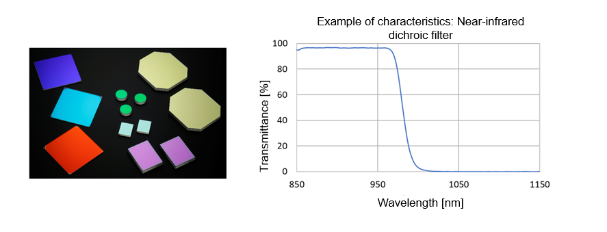
Dichroic mirrors/dichroic filters
By using multilayer dielectric films with different refractive rates, these mirrors or filters can separate light in an arbitrary specific wavelength range into transmitted light and reflected light using light interference. They are used for fluorescence analysis, lighting, and spectrometers for astronomical observation.
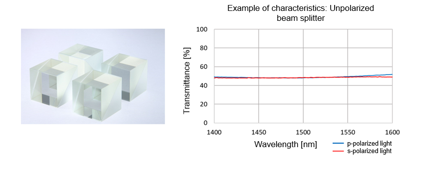
Beam splitters
A beam splitter can split light into two beams by reflectance and transmittance depending on the polarization component and intensity. There is a prism type and flat plate type. These beam splitters are used for optical pickups and optical communications.
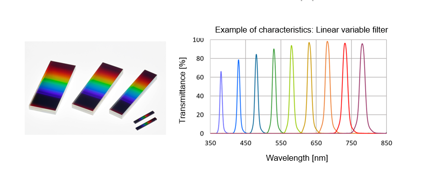
Linear variable filters
A linear variable filter is a linear, wedge-shaped optical filter coated on a single substrate, and its spectral characteristics vary linearly. The transparent wavelength can be adjusted by changing the position of the incident light. Linear variable filters are used in compact spectrometers due to their high wavelength resolution.
In addition to the products introduced above, we can design and manufacture band pass filters, notch filters, ND filters, metal coatings, etc. with ranges from ultraviolet through far-infrared and terahertz. We also offer products with custom specifications to meet customer needs, including not only spectral characteristics but also high laser resistance and value-added services such as direct coating on patterned wafers.
Application area
Mid-infrared and far-infrared rays
Infrared optical thin films are used as infrared sensors in a variety of applications, mainly in the fields of crime prevention, security and industrial equipment. Although there is no clear definition for the wavelength division of infrared rays, we define near-infrared as the region having a wavelength between 0.7 to 3.0 μm, mid-infrared between 3 to 8 μm, and far-infrared between 8 to 15 μm.
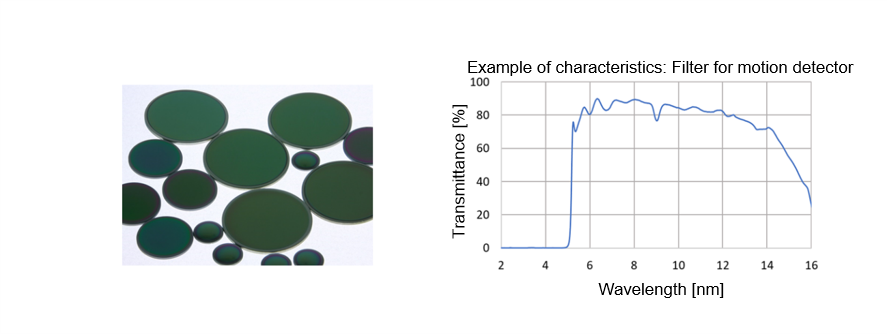
Filters for motion detectors
All objects emit infrared rays, and the temperature of the object determines the amount of radiation. For example, a human body at a temperature of about 37°C emits infrared rays with a maximum radiation dose of about 9 to 10 μm. By combining a pyroelectric element with a filter that efficiently transmits infrared rays of 9 to 10 μm, the element is used as a motion detector.
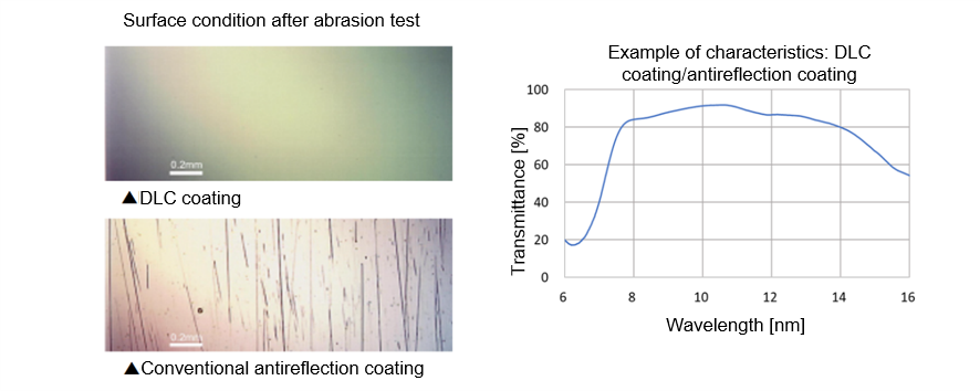
DLC coating
Environmental resistance is required for outdoor sensors, and the same applies to filters; high hardness, abrasion resistance, moisture resistance, and corrosion resistance are required of filters. To meet these requirements, diamond-like carbon (DLC) coating were developed. DLC coating used to be one of the surface treatment technologies to prolong the life of tools, but now these films can be used as optical filters due to their improved infrared transmission performance. With a refractive rate of 2 to 2.4, DLC coating can also be used as materials for antireflection films with regards to germanium and silicon used in infrared substrates. When an infrared camera is used in a harsh environment such as a beach or highway, an infrared window with a DLC coating on the outer surface and a broad antireflection coating on the opposite surface can be used.
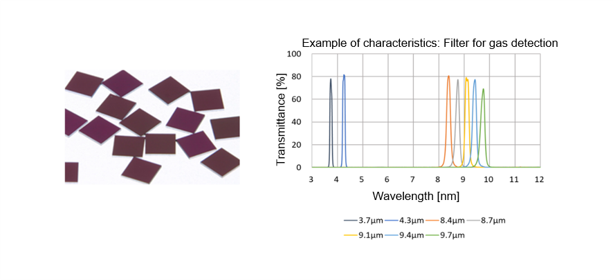
Filters for gas detection
There are intrinsic absorption spectra of various gases in the infrared band. By measuring the amount of absorption at the maximum wavelength of the absorbance in the intrinsic absorption spectra, it is possible to identify the components and analyze their concentrations. This method is called infrared absorption analysis and uses a bandpass filter that efficiently transmits only the maximum wavelength. For example, carbon dioxide has a maximum wavelength of around 4.26 μm. For a sensor that detects carbon dioxide, a filter that transmits a wavelength of 4.26 μm and blocks the other unwanted bands (from visual light range to around 11 μm) is used.
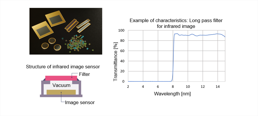
Filters for infrared image sensors
The heart of an advanced surveillance system is its infrared cameras, and cooled image sensors using mercury-cadmium-telluride (MCT) elements have been used for many years. Cooled image sensors are extremely sensitive, but the enclosures must be kept in a vacuum and at a low temperature to reduce thermal noise. In the 2000s, non-cooled image sensors that can operate even at room temperature were developed using microbolometers. They have become smaller and less expensive, and have come to be used in a wide range of fields such as home appliances, crime prevention, security, medical care, and automobiles. Compared with the filters for motion detectors described above, the filters required for infrared image sensors are characterized by a wider cutoff band and a wider and higher transmittance band from around 8 μm. Cooled image sensors must also maintain their performance at low temperatures. The outer periphery of a filter including its sides is coated with a solder-bonding metal for vacuum sealing. Depending on the object, a bandpass filter with a narrowed transmission band is used at the same time. For example, if you use a bandpass filter that matches the absorption spectra of a toxic gas, you can image the toxic gas. Not only can it detect toxic gas leaks, but it can also identify where leaks are occurring. In recent years, there has been active development of software to analyze and store data collected by sensors and utilize it as big data, as well as algorithms for increasing the resolution of images. At commercial facilities and train stations, we collect data on the number of visitors and their traffic lines, utilizing this data for marketing and evaluating congestion.
Ultraviolet rays (UV-C)
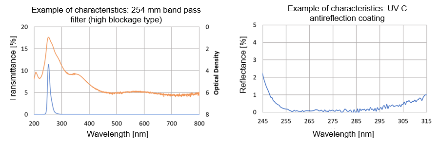
Among ultraviolet rays, the wavelength band shorter than 280 nm is called UV-C. In daily life, UV-C light is absorbed by the ozone layer and cannot reach the ground, but it is commonly used in the field of sterilization and semiconductors.
Sterilization band pass filters and antireflection coatings
The absorption spectrum of DNA and RNA (nucleic acid) in cells has an absorption maximum at around 260 nm. When bacteria or viruses are irradiated with ultraviolet rays at around 260 nm and nucleic acids absorb light, the nucleic acids are damaged and cell division is inhibited, thereby resulting in death. Optical thin film products in the field of sterilization include antireflection coatings that efficiently transmit light and bandpass filters that can block unwanted wavelengths.
Conceptual image of nucleic acids damaged by UV light
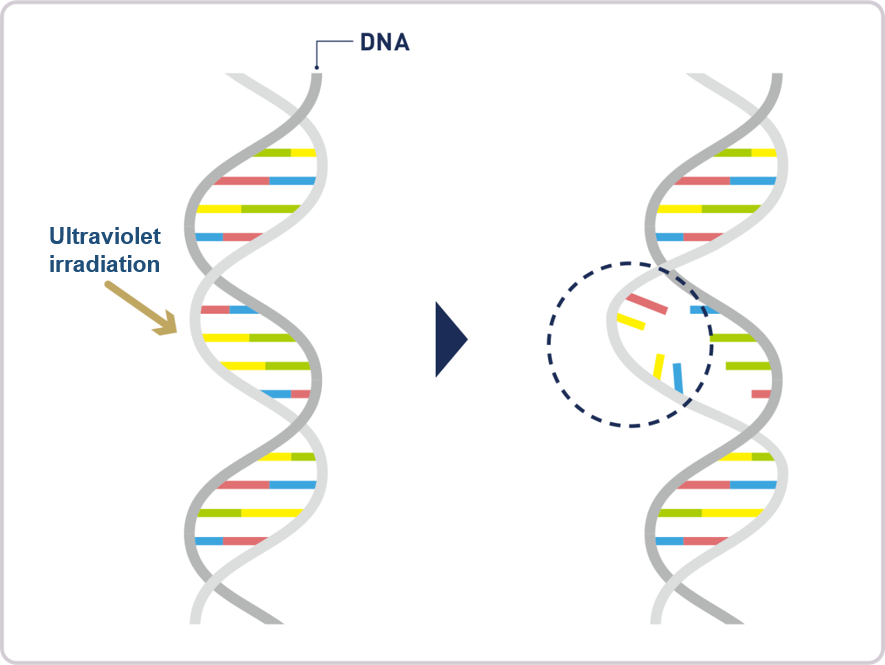
Nucleobases that make up nucleic acids absorb ultraviolet rays and the double helix structure is broken.
When the structure is broken, it becomes impossible to read the genetic information correctly from the nucleic acid.
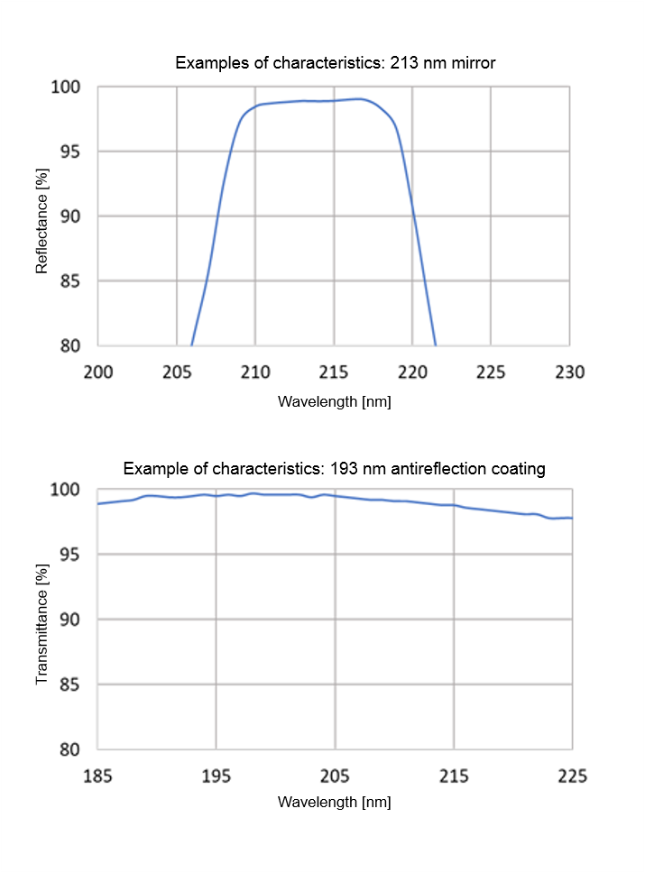
Mirrors and antireflection coatings for DUV light sources
Among UV-Cs, light around 200 nm is called DUV (Deep Ultraviolet) and is used as a light source for defect inspection systems for mask blanks and photomasks in semiconductor manufacturing processes. Since defects in mask blanks and photomasks greatly reduce yields on wafers after exposure, defect inspection systems are essential. Antireflection coatings and folded mirrors for DUV light sources are used in defect inspection systems.
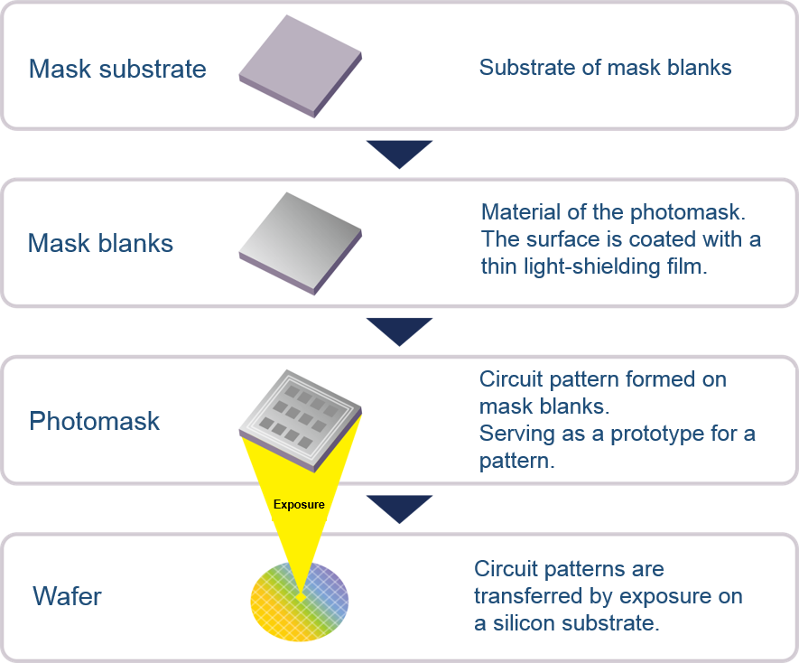
Conceptual image of semiconductor manufacturing process