Micro Lens Arrays and Fiber Array Units in Co-Packaged Optics
— Design Points for Improving Optical Coupling Efficiency
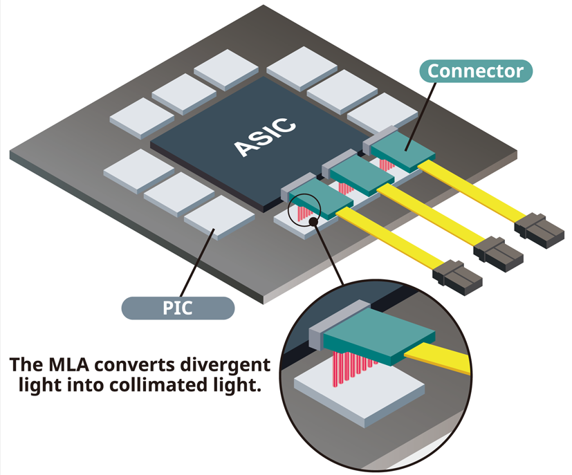
Communication bandwidth around switches and processors in data centers is rapidly increasing, driven by the expansion of AI workloads and other factors. In response to this growing bandwidth demand, conventional electrical wiring is reaching clear limitations in terms of both transmission distance and power consumption, making a shift to optical interconnects essential. Co-packaged optics (CPO) technology addresses this challenge by mounting optical engines directly on the package of a switch application-specific integrated circuit (ASIC). However, high overall system performance cannot be achieved simply by converting electrical signals into optical signals. Losses during the subsequent transmission process, particularly at optical coupling interfaces, have a major impact on power consumption and the overall link budget.
Among these, optical coupling between silicon photonics chips and fiber array units (FAUs) is one of the major sources of loss in CPO configurations. At this interface, multiple factors, such as mode size, numerical aperture (NA), and alignment accuracy are closely interconnected, and even slight mismatches can reduce coupling efficiency. As a result, even when high-efficiency light sources and devices are used, losses at the coupling interface can limit the performance of the entire system. Against this backdrop, optimizing optical coupling efficiency has become a critical design challenge in CPO systems.
Basic Overview of Optical Coupling Configurations in Co-Packaged Optics
Interface Between Silicon Photonics and Fiber Array Units
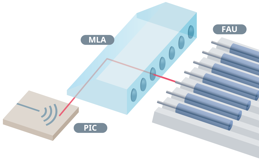
Optical coupling in CPO is established at the interface between the silicon photonics chip and the FAU. There are two main types of connection methods: grating couplers and edge couplers, each with distinct characteristics. Grating couplers emit light vertically from the chip surface, offering a high degree of flexibility in implementation. However, they have limitations in terms of coupling efficiency and bandwidth performance. By contrast, edge couplers transmit light horizontally, enabling high-efficiency and broadband transmission, but they require highly precise alignment.
In such optical interfaces, the FAU arranges multiple optical fibers with high precision and simultaneously connects multiple channels to the silicon photonics chip. In particular, because CPO systems are expected to support an increasing number of channels, collective coupling using an FAU has a significant impact on the overall system's implementation efficiency and performance.
Fiber Array Unit Structure and Features
An FAU is an optical component used to align and fix multiple optical fibers at a constant pitch, and its structure generally uses a V-groove substrate. These V-grooves define the fiber positions with high precision, enabling positioning accuracy on the order of micrometers. This mechanical accuracy is an important factor that directly affects optical coupling efficiency.
In addition, FAU fiber arrays are often based on standard specifications, such as a 127 µm pitch, ensuring compatibility with other optical components and assembly processes. Furthermore, many of the fibers used are single-mode fibers. Although their small mode field diameter requires high coupling efficiency, it also makes them highly sensitive to positional misalignment and NA mismatch. For this reason, an FAU should be designed not merely as a holding structure, but as an important interface that determines optical performance.
Role and Benefits of Introducing Micro Lens Arrays
Why Micro Lenses Are Necessary
When directly coupling a silicon photonics chip and an optical fiber, the biggest challenge is the mismatch in mode size. The waveguide mode on the chip side is extremely small, whereas a single-mode fiber has a larger mode field diameter. As a result, efficient optical transfer cannot be achieved as-is.
In addition, light emitted from the chip tends to diverge, and even a slight separation distance causes the beam diameter to expand, increasing coupling loss. To correct mode mismatch and beam divergence issues, the introduction of micro lenses is essential.
Basic Operation of Micro Lenses
Micro lenses play the role of shaping emitted light into an appropriate beam profile. Specifically, by converging or collimating a divergent beam, they form the optimal mode field diameter and wavefront for the target fiber or waveguide. This improves the optical mode overlap efficiency, or overlap integral, and reduces coupling loss.
In addition, the lens design makes it possible to control the NA of the beam, allowing it to be matched with the NA on the fiber side and reducing optical loss due to missed light or excessive divergence.
Effects of Introducing Micro Lens Arrays
By using micro lens arrays (MLAs) in combination with FAUs, optical coupling can be optimized for each channel, significantly improving the overall system's coupling efficiency. More importantly, controlling the beam profile with lenses increases tolerance to positional misalignment.
This enables designs that do not depend excessively on strict alignment accuracy, helping improve mountability and yield. As a result, MLAs are not merely a means of improving efficiency, but an important element that supports practical optical coupling design in CPO.
Key Parameters Related to Coupling Efficiency
Pitch Accuracy
In optical coupling, it is essential that the fiber array pitch of the FAU, the lens pitch of the MLA, and the pitch of the optical emission positions on the silicon photonics chip side are aligned with high precision.
If there is a mismatch in any of these elements, lateral positional misalignment occurs in each channel, reducing beam overlap. In particular, in multi-channel configurations, this misalignment has a cumulative effect that can significantly reduce overall coupling efficiency. Therefore, pitch accuracy should not only be optimized for individual components, but must be compatible across the entire system.
Lens Radius of Curvature
The radius of curvature of a micro lens is an important parameter that determines the focal length and directly affects coupling efficiency. In the event of an inappropriate curvature, the beam will not converge to the optimal size or position at the fiber end face, resulting in mode mismatch.
If the beam is focused too strongly, the beam diameter becomes too small and coupling efficiency decreases. Conversely, if the focusing is insufficient, the beam spreads too much and optical loss increases due to missed light. For this reason, lens design requires optimal focal design that takes into account the mode field diameter of the fiber and its placement position.
Numerical Aperture Matching
Matching the NA of the fiber and the lens is often overlooked, but it is an extremely important factor. If the beam aperture emitted from the lens is inappropriate for the fiber NA, the light will not be coupled into the fiber and will be lost.
If the NA is too small, only part of the light is coupled. If it is too large, the beam diverges and efficiency decreases. Single-mode fibers especially have a narrow allowable range, making NA design a dominant parameter that determines coupling efficiency.
Alignment Accuracy (XY, Z, and θ)
Alignment accuracy is also very important in optical coupling, and misalignment in the lateral direction (XY), optical axis direction (Z), and angle (θ) each affects coupling efficiency in different ways. Misalignment in the XY direction causes a mismatch in the beam center, while misalignment in the Z direction causes changes in beam diameter due to a shift in the focal position.
Angular misalignment changes the beam incidence conditions and becomes a major source of loss, particularly in edge-coupler configurations. These misalignments can have an individual impact, but when they occur in combination, losses increase further. Therefore, alignment design that takes allowable tolerances into account from the design stage is required.
Optimal Design Approach for Micro Lens Arrays and Fiber Array Units
Design Flow from a Practical Perspective
Mode Analysis
In mode analysis, the beam characteristics of the light emitted from the silicon photonics chip are accurately identified. Specifically, parameters such as mode field diameter, divergence angle, and wavefront shape are evaluated to quantitatively characterize the externally emitted beam. Insufficient understanding at this stage can lead to deviations throughout the subsequent design process. Therefore, analysis using actual measurements and high-precision simulations is important.
Lens Analysis
Next, during lens design, the radius of curvature, focal length, and placement position of the micro lens are determined based on the beam characteristics obtained through mode analysis. At this stage, it is necessary to achieve optimal beam shaping while ensuring compatibility with the mode field diameter and NA of the fiber. Rather than simply focusing the beam, it is important to create a configuration that is robust against assembly variations by taking alignment tolerances into account.
Fiber Array Unit Integration
Finally, in FAU integration, overall optimization is carried out, including the positional relationship and pitch between the designed micro lens and the FAU. The fiber array of the FAU, the lens array, and the emission positions on the chip side are aligned to achieve stable coupling efficiency for each channel. In this process, it is important to emphasize consistency across the entire system rather than optimizing each individual element separately.
Trade-Off Overview
In optical coupling design, multiple parameters interact with one another, making it essential to manage the associated trade-offs. For example, designs that maximize coupling efficiency generally result in tighter tolerances, increasing the difficulty of manufacturing and assembly.
In addition, setting a higher NA can improve light collection efficiency, but it also tends to increase sensitivity to beam divergence and positional misalignment, reducing alignment tolerance. Thus, balancing high efficiency with ease of implementation becomes an important consideration in practical design.
Implementation Considerations
Optical characteristics optimized at the design stage can also change significantly during the assembly process. In particular, during bonding and sealing processes, material shrinkage and stress may cause positional misalignment, affecting coupling efficiency.
Thermal expansion differences caused by temperature fluctuations also cannot be ignored and can affect long-term reliability and stability. Therefore, a total design approach is required, covering not only optical design but also materials, structure, and process conditions. By designing with implementation-related effects in mind from the start, it is possible to suppress performance variations during mass production.
AGC's Micro Lens Arrays Enable High-Precision and Flexible Optical Coupling
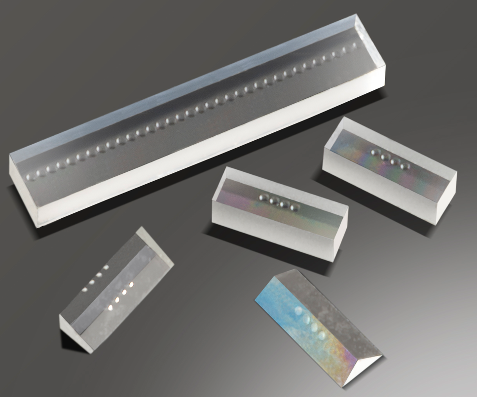
AGC's MLAs are optical components that integrate multiple microscale lenses with high precision. They provide functions such as collimation, coupling to optical fibers and waveguides, and light diffusion. Thus, they contribute to improved optical system performance and higher integration density.
Technical Features
Submicron-level high-precision lens profile processing enables excellent optical performance and stability. In addition, AGC's MLAs support high-precision pitch control and fine arrays within several tens of micrometers, making high-density integration possible. They also support single-sided and double-sided structures, as well as anti-reflection coatings, achieving both improved optical coupling efficiency and design flexibility.
Support for Custom Design
AGC also supports multi-row layouts and prism integration, providing flexible custom designs that enable complex optical requirements and advanced beam control.