Comprehensive Guide to Optical Waveguides: From Fundamentals to Material Design
Optical waveguides are components that enable light to be controlled and transmitted efficiently, and they are attracting attention across a wide range of fields, including communications, sensing, and displays. They are essential for high-speed, low-power information transmission that overcomes the limitations of electrical wiring. They also enable the miniaturization and weight reduction of AR devices, and improve the performance of next-generation networks and optical sensors.
In particular, AR device design involves many challenges, such as achieving a wide field of view, a uniform display, and a sufficient eyebox. Designers must also ensuring material transparency and optimizing refractive index. Image clarity and color accuracy, along with lightweight and thin design, also directly affect comfort, while balancing cost and manufacturability remains critical.
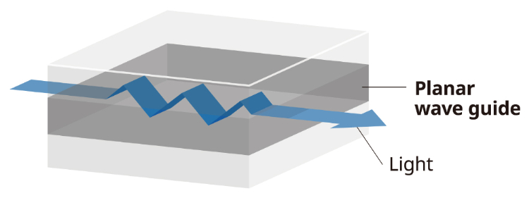
To meet these needs, planar waveguides—an applied form of optical waveguide technology—have become increasingly important in AR devices in recent years. The use of high-refractive-index materials is expected to enable wider fields of view and simpler structures.
Note: “Planar waveguides” refer to a type of waveguide structure formed on a flat substrate. For more information on waveguides, please see
Waveguide Materials | High-Refractive-Index Glass for AR/MR Glasses
Introduction to optical waveguides
What is an optical waveguide?
An optical waveguide is a structure that confines and guides light along a defined path by using differences in refractive index. In general, it consists of two or more layers—typically a core (higher refractive index) and a cladding (lower refractive index). Light propagates along the core while maintaining an intensity distribution determined by the refractive-index contrast.
Common waveguide configurations include slab, ridge, and channel types.
Why optical waveguides are attracting increasing attention
In recent years, optical waveguides have become increasingly important, particularly in the fields of information, communications, and sensing. As a technology that helps overcome the performance limits of high-speed electrical transmission, they are being actively researched and implemented across many application areas to meet the demands of next-generation networks.
- High-speed, energy-efficient data centers: Adoption of silicon photonics is accelerating to overcome the limitations of high-speed electrical interconnects
- Mobile and network infrastructure (5G/6G): As fronthaul and backhaul capacities increase, low-loss and highly reliable optical components are becoming increasingly important, with nitiatives such as the IOWN concept embodying these trends.
- AR glasses and displays: There is strong interest in the use of waveguides (including diffraction gratings) in thin and lightweight devices
Main applications of optical waveguides
Thanks to their high design flexibility and ease of integration, optical waveguides are being applied across a wide range of fields. Their use extends beyond communications to sensing, imaging, and industrial equipment.
- Communications: Intra-data-center optical interconnects, optical transceivers, optical switches, AWGs, filters, and couplers
- Sensing: Bio- and chemical analysis (waveguide interferometers, surface sensors), environmental monitoring, and LiDAR systems components
- Imaging and displays: Input/output diffraction gratings and waveguide layers for AR glasses
- Industrial equipment: Optical signal processing, laser light delivery, and optical path formation in measurement and inspection systems
Technical challenges in optical waveguide design
Reducing optical loss
The performance of an optical waveguide is determined by multiple factors, including scattering loss (surface and sidewall roughness), absorption loss (material-related), bending loss, and coupling loss (mode mismatch and misalignment). It is essential to optimize the following elements in an integrated manner by closely linking design with the manufacturing process:
- Control of core/cladding refractive indices and material uniformity
- Reduction of interface roughness between core and cladding during waveguide formation processes such as deposition and etching
- Optimization of bend radius and waveguide cross-sectional geometry
- Design of coupling optics for connected devices (optical fibers, light sources, displays), including tapers, gratings, and couplers
Manufacturing cost and mass producibility
A wide variety of manufacturing methods are used for optical waveguides, resulting in diverse process flows. Process choices such as photolithography, dry etching, nanoimprinting, and laser processing have a direct impact on cost and throughput.
Key factors for successful mass production include master mold fabrication, control of line-width variations, alignment accuracy, management of film thickness and refractive-index variations, and the introduction of in-line metrology. Depending on the application, choosing between wafer-based processes and integrated film or board molding approaches is essential to minimizing total cost of ownership (TCO).
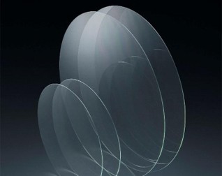
Material selection for optical waveguide design

In general, the use of glass in optical waveguides is relatively limited. In practice, silica-based and polymer-based materials are more commonly adopted, and the realistic approach is to select materials based on environmental conditions, required performance, and cost.
To provide an overview of each material's characteristics, we have prepared the comparison table below. We also outline how to identify the optimal solution based on these properties.
■ Comparison of material properties
| Material | Low-loss characteristics | Processability | Environmental resistance | Cost |
|---|---|---|---|---|
| Glass-based | 〇 | 〇 | ◎ | △ |
| Silica-based | ◎ | △ | ◎ | △ |
| Polymer-based | △ | ◎ | 〇 | ◎ |
Glass-based materials
Glass-based materials play an important role in optical waveguides where high stability and low loss are required. They are particularly effective in applications that demand resistance to harsh environmental conditions and long-term stability.
Advantages
- Low loss and high stability: Absorption is minimized through composition control, providing stability against temperature, humidity, and chemical environments
- High dimensional and refractive-index uniformity: Variation in properties along the propagation direction are minimized
- High hermeticity: Well suited for sealing and packaging applications
Disadvantages / considerations
- Patterning difficulty and cost: Fine patterning and high-aspect-ratio structures depend heavily on equipment and process capabilities, often resulting in higher costs.
Typical applications
- Light-guiding paths in industrial, outdoor, and automotive sensors and in chemical analysis equipment
- Devices requiring stable visible-light propagation and input/output optics, such as waveguide components for AR/MR glasses
- Optical modules requiringe miniaturization and tight bend radii while prioritizing long-term stability
By using high-refractive-index glass, the refractive-index contrast between the core and cladding can be increased, enhancing optical confinement within the same cross-section. This helps reduce bending loss and shrink device footprints. At the same time, careful evaluation of design flexibility and cost trade-offs is essential.
Silica-based materials
Silica (quartz) materials are the most standard and widely used optical waveguide materials, known for their high reliability. They offer excellent optical transparency and chemical stability, with particularly low loss in telecommunications wavelength bands (especially 1.3–1.55 μm).
Advantages
- Ultra-low loss and high transparency: Extremely low optical absorption in the 1.55 μm band, ideal for long-distance transmission
- Thermal and chemical stability: Minimal property changes at high temperatures and excellent resistance to moisture and chemicals
- Mature manufacturing processes: Established technologies derived from optical fiber and semiconductor fabrication, providing high reproducibility and reliability
- Refractive-index controllability: Precise refractive-index design enabled through doping (e.g., Ge, P, B)
Disadvantages / considerations
- Processing difficulty and cost: Requires high-temperature processes such as plasma CVD and flame heating, leading to higher capital and process costs
- Limitations in miniaturization and high integration: Low refractive-index contrast tends to result in larger bend radii
- Limited throughput: Deposition and thermal treatments can be time-consuming, reducing mass-production efficiency
Typical applications
- PLCs (Planar Lightwave Circuits) and AWGs (Arrayed Waveguide Gratings) for optical communications
- High-precision interferometers, optical sensors, and spectroscopic measurement systems
- Laser interferometry and optical frequency combs for research applications
- Optical modules requiring high reliability for space, defense, and infrastructure monitoring
Polymer-based materials
Polymer-based materials offer excellent processability and suitability for mass production, enabling cost-effective waveguide implementations. Their compatibility with flexible substrates has also attracted attention for board-level interconnects and mobile device applications.
Advantages
- Excellent processability and mass-production capability: Large-area, low-cost fabrication using nanoimprint and photolithography techniques
- Compatibility with flexible substrates: Can be formed on boards or films, making them suitable for short-distance optical interconnects
- Design flexibility in refractive index: Wide refractive-index tuning is possible through material design
Disadvantages / considerations
- Moisture absorption and thermal properties: Refractive-index and dimensional changes caused by humidity and temperature, challenging for long-term stability
- Chemical and UV resistance: Degradation countermeasures may be required depending on the application
Typical applications
- Light-guiding paths in industrial, outdoor, and automotive sensors, and in chemical analysis equipment
- Board-level optical wiring and short-reach interconnects in data centers
- Waveguides and diffractive elements for AR/VR/MR displays, leveraging lightweight and large-area formability
High-refractive-index glass from AGC
AGC’s high-refractive-index glass can be an effective option for specific waveguide applications from the perspectives of miniaturization, suppression of bending loss, and environmental stability. In particular, it offers strong potential in the following use cases:
- Equipment requiring long-term stability under harsh environments (high temperature, high humidity, chemical exposure)
- Analytical and measurement instruments that require stable light guiding from the visible to near-infrared range
- Compact optical modules with strict constraints on bend radius
Features
- High refractive index: Strong mode confinement contributes to the miniaturization of optical components
- Material uniformity: Minimal refractive-index variation in both thickness and in-plane directions, enabling designs that closely match target specifications
- Environmental resistance: Small performance variations under temperature/humidity fluctuations and chemical environments
Key considerations for implementation
- Quantitative comparison based on target specifications (loss, wavelength, bend radius, temperature/humidity conditions, and TCO)
- Hybrid configurations with polymers (e.g., using glass only for input/output or bus waveguides)
- Evaluation of processing and sealing methods (laser processing, etching, bonding)
Product Inquiries & Information Requests